Certified by
Capabilities

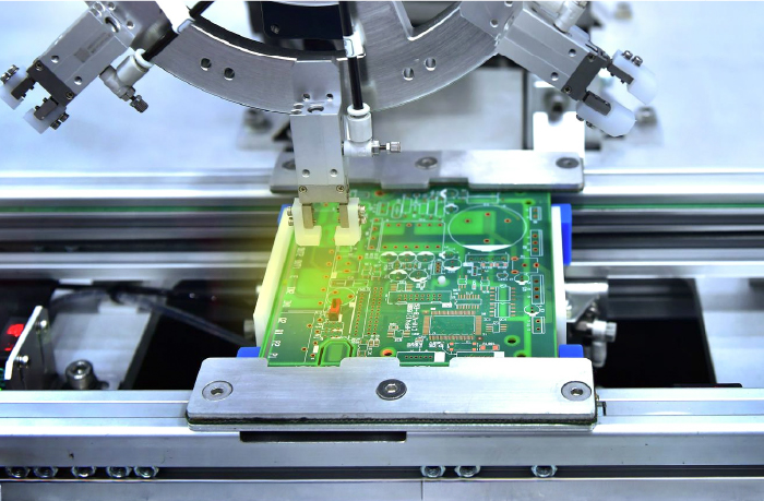
Cutting-Edge HDI PCB Manufacturing for Medical Technology

Delivering advanced HDI circuit boards designed for medical innovations, ensuring exceptional precision, reliability, and consistent performance across demanding healthcare applications worldwide.

introduction

Trusted HDI PCB Production for Medical Equipment.

Engineered for healthcare applications, our HDI boards deliver outstanding precision, stability, and long-term reliability. Advanced processes and strict quality control ensure consistent performance, supporting complex designs required in critical and high-performance medical systems.

capabilities

Our HDI PCB Manufacturing Capabilities

Specifications PCB Capabilities
PCB Layers 4 ~40 layers
High-Density Layers Up to 36 layers
Delivery Time 1 day to 3 weeks
Stackup 1+n+1,1+1+n+1+1,2+n+2,3+n+3(n buried vias≤0.3mm),Laser blind via can be filling plating
PCB Via Blind via, Buried via, Staggered via, Stacked via, Skip via
Minimum Laser Drill Diameter 0.1mm
Final PCB Thickness 0.4-10mm
Min BGA Pad Size  HASL:10mil, LF HASL:12mil, other surface technics are 10mil(7mil is ok for flash gold)
Copper Thickness 1/2oz - 10oz
Surface Finishes ENIG, Hard gold, Flash gold, HASL Lead free, OSP, ENEPIG, Soft gold, Immersion silver, Immersion Tin
Materials Megatron 6&7, Shengyi S1000-2, Rogers 4350B, 4003C, 6035HTC, TU768, 370HR, FR408, IT180
Impedance Control ±5ohm(<50ohm), ±10%(≥50ohm)
Max. Board Size 500*600mm(19''*23'')
Silkscreen White, Black, Red, etc.
Soldermask Green, Blue, Purple, White, Black, Pink, Orange

Get Instant Quote

Advantages

Why You Choose Our HDI PCB

  • Advanced Equipment

    Our HDI PCB production facility is equipped with advanced machinery that ensures precise microvia drilling, fine-line etching, and accurate multilayer alignment. Each process is carefully controlled to meet the tight tolerances required for high-density designs.

    From automated optical inspection to high-speed lamination and plating, our equipment guarantees consistent quality, signal integrity, and reliability. This allows us to support complex medical, wearable, and high-performance electronics applications with efficiency and precision.

    Get Instant Quote
  • Strict Quality Control

    We implement strict quality control throughout the HDI PCB manufacturing process to ensure every board meets the high reliability standards required for medical applications. Automated optical inspection, flying probe testing, and impedance verification detect defects early, maintaining consistent performance across complex, high-density designs used in medical devices.

    In addition, mechanical and thermal testing validate durability under demanding conditions. By combining advanced inspection methods with rigorous process monitoring, we guarantee HDI PCBs that deliver long-term stability, precision, and reliability for critical medical equipment, wearable health devices, and other high-performance healthcare electronics.

    Get Instant Quote
  • DFM Support for Medical HDI PCBs

    Our expert engineering team provides comprehensive Design for Manufacturability (DFM) support, helping optimize HDI PCB layouts for bend areas, trace routing, and multilayer stack-ups. This ensures efficient production and minimizes defects from the earliest design stage.

    With DFM guidance, medical device designs—such as wearable monitors, diagnostic equipment, and implantable devices—achieve maximum reliability and precision, reducing development risks and accelerating time-to-market for critical healthcare applications.

    Get Instant Quote
  • Fast Lead Time & Flexible Production

    We offer rapid prototype turnaround, typically within 5–7 days, and flexible production options for small or large volumes. Our streamlined processes ensure timely delivery without compromising quality.

    This agility supports medical device projects, from wearable health monitors to diagnostic equipment, allowing quick iterations and reliable mass production. By combining speed with precision, we help healthcare innovators bring critical devices to market faster and more efficiently.

    Get Instant Quote
testimonials

Hear from Our Customers

  • “The HDI PCBs delivered exceptional precision and reliability, allowing our implantable devices to operate safely and efficiently over long-term use.”

    Dr. Hannah Lee

    iomedical Engineer

  • “Their HDI solutions supported our complex multi-layer designs, ensuring signal integrity and durability critical for high-performance diagnostic systems.”

    Michael Roberts

    R&D Manager, Medical Equipment

  • “Working with their team, we optimized our HDI PCB design for compact wearables. The results were reliable, consistent, and fully met medical standards.”

    Sarah Wang

    Product Development Lead, Wearable Health Tech

  • “On-time delivery, strict quality control, and stable performance make their HDI PCB production a dependable part of our medical device supply chain.”

    James Patel

    Supply Chain Director, Medical Devices

Faqs

Frequently Asked Questions

Explore answers to common questions about our HDI PCB manufacturing capabilities, including precision, layer density, reliability, and suitability for complex applications. This helps clients quickly understand our technical strengths and production expertise.

1. What is the maximum layer count supported for HDI PCBs?
We can manufacture HDI PCBs with up to 36 layers, allowing for complex, high-density interconnections required in advanced applications like medical devices and aerospace electronics.
2. What is the minimum line width and spacing achievable in HDI designs?
Our HDI process can achieve a minimum line width and spacing of 50μm / 50μm, supporting fine-pitch components and high-density routing for compact, high-performance designs.
3. Can you produce HDI PCBs for high-reliability applications like medical devices?
Yes. Our HDI PCBs meet IPC Class 2 and Class 3 standards, ensuring mechanical durability, signal integrity, and long-term reliability for critical healthcare applications.
4. What types of microvias and advanced interconnects are available?
We support blind vias, buried vias, stacked microvias, and laser-drilled microvias, enabling multi-layer interconnections and high-density layouts while maintaining signal performance.
5. How do you ensure consistent quality and signal integrity for HDI PCBs?
Through strict quality control, including AOI, flying probe testing, impedance testing, and thermal/ mechanical validation, we guarantee high performance, reliability, and repeatability for every HDI PCB produced