Medical Multilayer PCB

We manufacture high-reliability multilayer PCBs for life-critical medical devices. Our advanced layer-count capabilities and certified quality standards ensure maximum signal integrity and precision for complex medical electronics.

• ISO 13485, ISO 9001 & IPC-A-610 Class 2/3 Compliant
• Up to 40-Layer Rigid, 8-Layer Flex & 20-Layer Rigid-Flex
• In-stock High-Reliability Materials Including Shengyi, Panasonic & Rogers

Medical Multilayer PCB
Certifications
What is Medical Multilayer PCB
introduction

What is Medical Multilayer PCB?

A medical multilayer PCB features three or more copper conductor layers laminated together with high-grade insulating materials. By interconnecting these internal layers with plated through-holes, blind vias, and buried vias, we build highly compact, complex circuits that fit high-density electronics into smaller form factors. This advanced construction is essential for modern medical devices, delivering the high signal integrity, precise routing, and rugged reliability required for diagnostic tools, imaging systems, patient monitors, and life-critical equipment.

Products
 

Advantages of Medical Multilayer PCB

  • Higher Routing Density
  • Better Power Distribution
  • Exceptional Mechanical Reliability
  • Reduced Signal Noise & Enhanced Grounding
Higher Routing Density
Stacking three or more conductive layers dramatically increases circuit density while shrinking the total board footprint. This makes multilayer PCBs essential for portable diagnostic tools, wearable patient monitors, and space-constrained medical devices.
Better Power Distribution
Exceptional Mechanical Reliability
Built with advanced laminates and engineered to resist heat, vibration, and thermal expansion, these boards maintain structural integrity over time. Supporting rigid, flex, and rigid-flex options, they offer the mechanical resilience required for demanding healthcare environments.
Reduced Signal Noise & Enhanced Grounding
Why Choose Us

Choosing MedPCB as Medical Multilayer PCB Partner

  • ISO 13485 Certified & Medical-Grade Materials

    ISO 13485 Certified & Medical-Grade Materials

    Our facility operates strictly under ISO 13485 certified quality management and IPC Class 2/3 assembly standards. We source high-performance, medical-grade laminates including Rogers, Panasonic, and Shengyi, ensuring every multilayer board complies with global regulatory and life-safety requirements.

  • Strict Impedance Testing & Control

    Strict Impedance Testing & Control

    We perform precise controlled impedance testing matched to your specific stackup layout and layer counts ±8% for Standard, ±5% for High Precision. By managing differential pairs, trace widths, and dielectric spacing, we guarantee optimal signal integrity, low loss, and zero interference for sensitive medical diagnostics and imaging gear.

  • Free DFM Engineering Support

    Free DFM Engineering Support

    MedPCB PCB engineers perform a thorough Design for Manufacturability (DFM) review on every order prior to production. We spot layout errors, signal path conflicts, and thermal issues early, helping you prevent costly redesigns, lower manufacturing costs, and speed up time-to-market.

  • Free Via-in-Pad Support for HDI Designs

    Free Via-in-Pad Support for HDI Designs

    We offer complimentary Via-in-Pad technology for multilayer medical designs. By filling and capping vias directly beneath component pads, we maximize routing area, reduce parasitic inductance, and allow for ultra-compact BGAs without extra engineering fees.

  • Sterile Packaging & Full Lot Traceability

    Sterile Packaging & Full Lot Traceability

    To safeguard product purity, all assembled medical PCBs undergo rigorous final cleaning and are sealed in contamination-free, ESD-safe sterile packaging. Combined with our MES tracking systems, we maintain complete lot-to-lot material traceability for total regulatory compliance.

Specs

Technical Specification

Layer Count

4–40 layers

Maximum Board Size

Standard: 500 × 600 mm (19" × 23")

Advanced: 1100 × 500 mm (43" × 19")

Base Materials

High-Tg FR4, Rogers, Polyimide, Megtron, Taconic, Arlon

Via Technology

Blind & Buried Vias, Microvias, Via-in-Pad, Back Drilling

Impedance Control

±8% (Standard), ±5% (High Precision)

Layer Registration

4 Layers: 0.15 mm / 0.10 mm (Std./Adv.)

6 Layers: 0.20 mm / 0.13 mm

8 Layers: 0.25 mm / 0.15 mm

Minimum Clearance

Hole Edge to Inner Circuit: 0.225 mm / 0.15 mm 

Board Outline to Inner Circuit: 0.38 mm / 0.225 mm

Minimum Board Thickness

4 Layers: 0.30 mm / 0.20 mm (Std./Adv.)

6 Layers: 0.60 mm / 0.50 mm

8 Layers: 1.00 mm / 0.75 mm

Thickness Tolerance

4 Layers: ±0.13 mm / ±0.10 mm (Std./Adv.)

6 Layers: ±0.15 mm / ±0.13 mm

8–12 Layers: ±0.20 mm / ±0.15 mm

Surface Finishes

ENIG, ENEPIG, Immersion Gold, Immersion Silver, Immersion Tin, OSP, Hard Gold

Solder Mask Colors

Green, Black, Blue, Red, White, Yellow, Purple (Matte or Glossy)


Medical Multilayer PCB
Capabilities

MedPCB Medical Multilayer PCB Process

Step 1: Design & Stackup Review
Our engineering team performs a comprehensive Design for Manufacturability (DFM) and signal integrity review of your layer stackup. We optimize track spacing, dielectric thickness, and layer ordering to eliminate cross-talk, prevent board warping, and ensure flawless performance in critical healthcare environments.
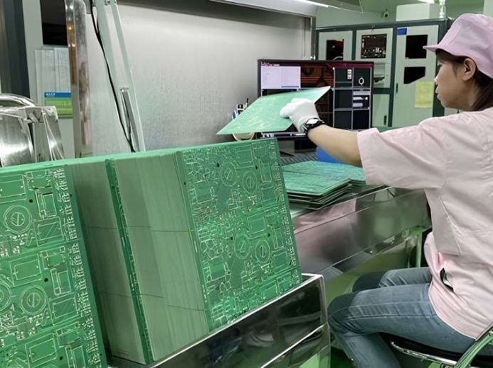
Step 2: Inner Layer Imaging & Etching
Step 3: Lamination & Drilling
Step 4: Outer Layer Imaging, Plating & Surface Finish
Step 5: Electrical Testing & Final Inspection

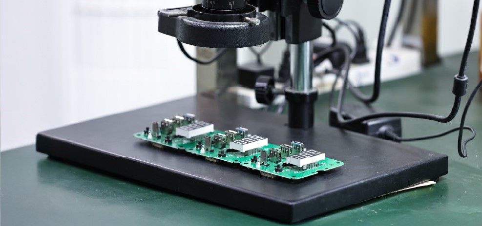
Every multilayer board undergoes exhaustive quality testing to guarantee 100% layer-to-layer connection accuracy and structural integrity before leaving MedPCB:


Microsectioning & Cross-Section Analysis to verify dielectric thickness and via plating uniformity
AOI (Automated Optical Inspection) for inner and outer layer trace precision
X-Ray Inspection to verify layer alignment and registration
Electrical Flying Probe & Bed-of-Nails Testing for shorts and open circuits
• Controlled Impedance Testing to validate high-frequency signal paths

Quality Control

Common Challenges in Medical Multilayer PCB Manufacturing

  • Substrate & Stack-Up Matching

    Substrate & Stack-Up Matching

    Challenge: Asymmetric stack-ups or mismatched materials cause thermal stress, resulting in board warping, bow-and-twist defects, and trace cracking during high-temperature reflow.

    Our Solution: We manufacture strictly balanced, symmetrical stack-ups using high-grade, thermally matched laminates (Rogers, Panasonic, Shengyi) to ensure flat, structurally stable boards.

  • Strict Inner-Layer Impedance Control

    Strict Inner-Layer Impedance Control

    Challenge: Micro-variations in trace width, copper thickness, or dielectric spacing on inner layers cause signal attenuation and electromagnetic interference (EMI).

    Our Solution: We enforce tight manufacturing tolerances using automated etching lines and perform 100% controlled impedance testing across all signal layers for noise-free transmission.

  • High Lamination Complexity

    High Lamination Complexity

    Challenge: Laminating high-layer-count boards risks resin starvation, micro-voids, and layer misregistration, causing electrical opens or shorts.

    Our Solution: We utilize advanced vacuum lamination presses with precise heat and pressure controls to guarantee uniform bonding, zero void formation, and precise layer registration up to 40 layers.

  • Design for Manufacturability (DFM) Challenges

    Design for Manufacturability (DFM) Challenges

    Challenge: High-density layouts with microvias, blind/buried vias, and IPC Class 3 specs often contain hidden manufacturability errors that delay production.

    Our Solution: We provide complimentary DFM analysis to review your Gerber files, verify trace clearances, check via structures, and ensure your layout is fully production-ready before manufacturing begins.

Cost Considerations for Medical Multilayer PCBs
Specs

Cost Considerations for Medical Multilayer PCBs

Medical-grade multilayer PCBs require high precision. We manufacture high-precision medical-grade multilayer PCBs and help balance cost, compliance, and reliability for your projects.

• Layer Count & Size - Increasing the number of PCB layers requires additional lamination, drilling, alignment, and inspection processes. Medical devices often demand controlled impedance, dense routing, and tighter manufacturing tolerances, making high-layer-count boards more complex and costly to produce.

• Materials & Vias - Standard FR-4 and traditional plated through-holes are the most economical choices. Upgrading to high-frequency laminates (like Rogers) or complex blind/buried microvias requires extra manufacturing cycles, raising overall expenses.

• Finishes & Delivery - Basic HASL is low-cost, but medical devices often need ENIG or ENEPIG for flatness and biocompatibility, which increases finish costs. You can offset these costs by ordering in larger production volumes and avoiding rush fees through standard lead times. 

MedPCB supports your medical multilayer PCB projects with material recommendations, free DFM review, and IPC Class 2/3 manufacturing for reliable, cost-effective production. Just send us your Gerber file today!


Case Study

Medical Multilayer PCB Case Study

  • Tonometer
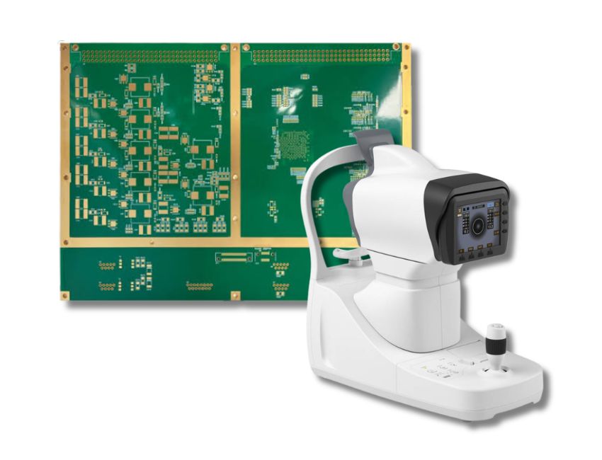
    Tonometer PCB  Tonometer

    Tonometer PCB 

    High-precision 6-layer PCB designed with dedicated inner shielding layers to isolate sensitive analog sensor signals from external noise, ensuring accurate intraocular pressure readings.

  • Nurse Station Terminal
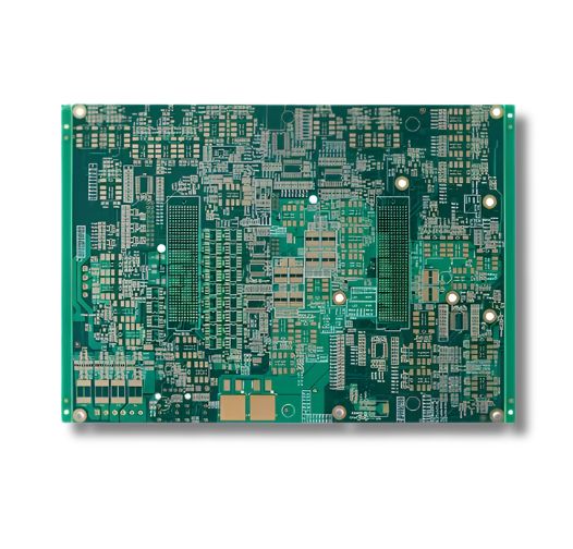
    Nurse Station Terminal PCB  Nurse Station Terminal

    Nurse Station Terminal PCB 

    High-density 8-to-10-layer PCB stackup featuring controlled impedance and integrated power/ground planes to support continuous high-speed data transmission and multi-device connectivity.

  • Surgical Headlamp
    Surgical Headlamp PCB  Surgical Headlamp

    Surgical Headlamp PCB 

    Thermal-optimized 4-layer metal-core PCB designed with heavy copper layers and strategic thermal vias to efficiently dissipate heat away from high-power LEDs in compact wearable housings.

  • RVG Sensor
    RVG Sensor Multilayer PCB  RVG Sensor

    RVG Sensor PCB 

    Ultra-thin, ultra-flexible 4-layer rigid-flex PCB engineered with micro-vias and high-density interconnect (HDI) technology for tight space constraint, fast intraoral X-ray data transfer, and moisture resistance.

Faqs

Frequently Asked Questions

Our Medical Multilayer PCB FAQ addresses essential questions regarding your manufacturing requirements. We cover our capabilities for complex medical electronics, supply chain management, assembly timelines, rigorous quality inspection protocols, and our capacity to scale from initial builds to production batches. For every medical device project, we guarantee precision-focused, medical-grade assembly standards.

1. How Can You Distinguish Between Single-Layer And Multilayer PCBs?
Single-layer PCBs have conductive copper on only one side of a single substrate. A multilayer PCB uses three or more copper layers. Insulating dielectric material separates the layers, while plated vias create electrical connections between them..
2. Why Are Multilayer PCBs Used In Medical Devices?
Multilayer PCBs allow us to build compact, high-density designs necessary for advanced medical electronics such as imaging systems, implants, and IoT-enabled diagnostic tools.
3. What Types Of Substrates Do You Use For Medical PCBs?
We offer a wide range of high-reliability substrates depending on your application, including standard high-Tg FR4, PTFE, Polyimide, and advanced laminates from industry leaders like Rogers, Isola, Arlon, and Nelco.
4. Why is EMC Required For Medical PCBs?
Electromagnetic Compatibility (EMC) is mandatory to ensure a medical PCB limits its own electromagnetic emissions. It prevents interference with nearby equipment while maintaining total immunity to external electromagnetic noise.
5. How Are Thermal Properties Managed In Complex Multilayer PCBs?
We utilize high-Tg dielectric materials, heavy copper layers, strategic thermal via arrays, and specialized heat sinks to rapidly dissipate thermal loads, preventing delamination and ensuring long-term electrical stability.
6. How Does Your Medical PCB Fabrication Process Maintain Signal Accuracy?
We ensure low signal loss through tight controlled impedance manufacturing, High-Density Interconnect (HDI) microvia technology, optimized layer stackups, and precise dielectric spacing across high-frequency circuits.
7. Can Medical PCBs Be Customized For Compact Wearable Devices?
Yes. We fabricate ultra-compact rigid-flex and flexible PCBs that fold into tight spaces. These lightweight, durable designs are engineered specifically for continuous health monitoring and portable medical wearables.
8. How Do You Ensure The Sterilization Compatibility Of Medical PCBs?
We utilize robust, high-temperature substrates and specialized conformal coatings that withstand harsh sterilization environments including autoclaving, chemical wipe-downs, and gamma radiation.

9. What Future Trends Are Shaping Medical Multilayer PCB Technology?
Advanced technologies are transforming medical multilayer PCBs to make healthcare devices smaller, faster, and more reliable: 

• Advanced Materials & Thermal Management: Low-loss dielectrics and high-conductivity laminates enable high-frequency data streaming for real-time patient monitoring and high-power medical diagnostic equipment.
• HDI & Microvias: Sub-150-micron microvias allow extreme circuit miniaturization, paving the way for next-generation wearables, implantables, and compact surgical tools.
• Embedded Components: Placing passives directly inside inner board layers drastically shrinks device footprint while shortening signal paths for ultra-accurate vital sign readings.

Product Related