Medical Heavy Copper PCB

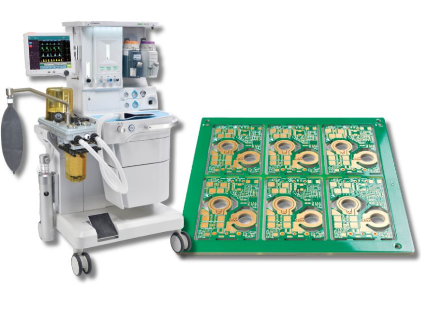
We manufacture high-reliability medical heavy copper PCBs designed for high-power, high-current healthcare applications. We support up to 100 oz, and mixed-copper weight configurations.

• ISO 13485, ISO 9001 & IPC Class 2/3 certified manufacturing.
• Up to 100 oz Copper Weight for extreme power and thermal management.
• Heavy, Extreme & Mixed Copper weight options available.

Medical Heavy Copper PCB
Certifications
What is Medical Heavy Copper PCB
introduction

What is Medical Heavy Copper PCB?

A medical heavy copper PCB is a printed circuit board built with copper weights ranging from 3 oz to 100 oz, to handle high current, reduce electrical resistance, and dissipate heat efficiently. Compared with standard PCBs, heavy copper boards provide lower electrical resistance, improved heat dissipation, and greater mechanical strength. They are widely used in medical power supplies, imaging systems, surgical equipment, and other healthcare devices that require stable electrical performance, efficient thermal management, and long-term reliability.

Products

Advantages of Medical Heavy Copper PCB

  • Superior Thermal Management
  • High Current Carrying Capacity
  • Enhanced Mechanical Durability
  • Mixed Copper Weight Capability
  • Excellent Reliability Under Continuous High Load
Superior Thermal Management
Thick copper layers act as built-in heat sinks, reducing operating temperatures by up to 20% compared to standard boards. This keeps critical high-power components running cool and extends the operational lifespan of sensitive medical devices.
High Current Carrying Capacity
Enhanced Mechanical Durability
Mixed Copper Weight Capability
Excellent Reliability Under Continuous High Load
Why Choose Us

Choosing MedPCB as Medical Heavy Copper PCB Manufacturer

  • ISO 13485 Certified Manufacturing

    ISO 13485 Certified Medical Manufacturing

    Our manufacturing facilities strictly comply with ISO 13485 standards and IPC-A-610 Class 2/3 guidelines. Every heavy copper PCB undergoes rigorous quality protocols to meet strict healthcare regulations and ensure life-critical device safety.

  • Free DFM Engineering Review

    Free DFM Engineering Review

    Our engineering team conducts a complimentary Design for Manufacturability (DFM) review on every project. We analyze trace spacing, copper weight balance, and thermal relief to identify design risks early, preventing costly production delays and re-spins.

  • Advanced Etching Techniques

    Advanced Etching Techniques

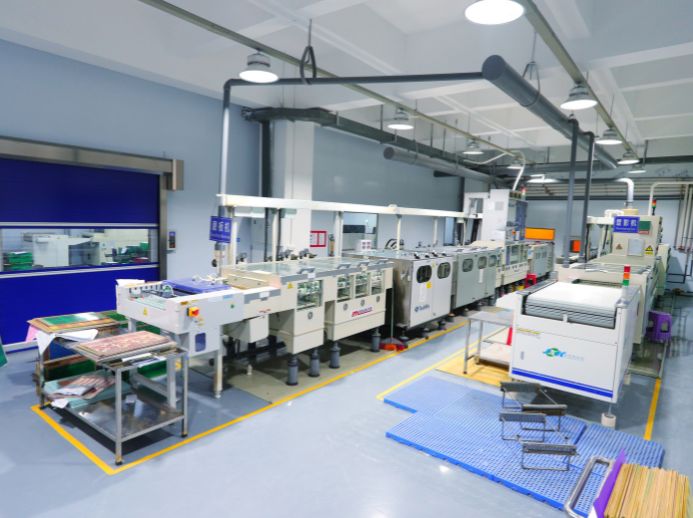
    Etching heavy copper structures requires extremely precise process control. MedPCB utilizes differential etching techniques to maintain accurate trace geometry across heavy copper designs, including projects requiring copper weights.

  • Up to 100 oz Heavy Copper Capability

    Up to 100 oz Heavy Copper Capability

    Capable of processing extreme copper weights from 3 oz to up to 100 oz, MedPCB supports ultra-high power density designs without compromising structural integrity. This extreme copper capacity allows custom medical hardware to deliver high-amperage power reliably within minimal physical footprints. 

  • High-Performance Substrate Selection

    High-Performance Substrate Selection

    Heavy copper PCBs demand substrates that withstand severe thermal expansion. We utilize high-Tg FR-4 and polyimide base materials engineered to improve thermal stability while minimizing warpage and delamination.

Specs

Technical Specifications

Process

Standard

Advanced

Copper Thickness


Minimum 1/2 OZ

Maximum 4 OZ

Minimum 1/3 OZ

Maximum 100 OZ

Layer


1–20 layers

22–40 layers

Material

Standard FR-4 materials, including KB, Shengyi, FR408, IS410, GETEK, 370HR, IT180A, and other common laminates.


High-performance materials such as Rogers, PTFE laminates, Taconic, Arlon, Nelco, and hybrid FR-4/RF laminates.

Finished Board Thickness

0.2–3.2 mm

3.4–10 mm

Minimum Tracking/Spacing 

Internal Trace/Space:
3oz Cu 5/8mil, 4 oz Cu 6/11mil, 10oz Cu 12/28 mil

External Trace/Space:
3oz Cu 6/12mil, 4 oz Cu 7.5/15mil, 10oz Cu 14/38 mil

Internal Trace/Space:
3oz Cu 5/8mil, 4 oz Cu 6/11mil, 10oz Cu 12/27 mil

External Trace/Space:
3oz Cu 6/10mil, 4 oz Cu 7.5/13mil, 10oz Cu 14/35 mil

Maximum Board Size


Up to 500 × 600 mm


Up to 1000 × 500 mm

Surface Finish

Standard lead-free & HASL finishes

Advanced finishes (Gold Finger, Hard Gold, ENIG+OSP)

Soldermask 


Green, Black, Blue, Red, White, Yellow, Purple Matte/Glossy

Via Process


Tenting Vias, Plugged Vias and Unplugged Vias

Testing


Fly Probe Testing, Electrical Testing (E-test) and AOI Testing

Technical Specifications
Capabilities

MedPCB Medical Heavy Copper PCB Process

Step 1: Material Selection & Preparation

Production begins by selecting the appropriate PCB substrate and copper foil based on the board's electrical, thermal, and mechanical requirements. For improved trace accuracy, heavy copper PCBs typically use thinner base copper before building up the required copper thickness through plating. 


Common substrate materials:


• FR-4 Standard - Tg 130-140°C for most applications
• High Tg FR-4 - Tg 170-180°C for high-temperature applications
• Polyimide - Tg 250°C+ for extreme environments
• Rogers/Ceramic for RF and high-frequency applications
Step 2: Heavy Copper Imaging & Controlled Etching
Step 3: Copper Build-Up Plating & Hole Metallization
Step 4: Surface Protection & Surface Finishing 
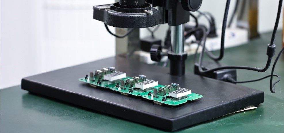
Step 5: Inspection, Testing & Quality Assurance
Quality Control

Challenges of Heavy Copper PCB Manufacturing 

  • Etching Thick Copper Layers

    Etching Thick Copper Layers

    Challenge: Etching thick copper up to 10 oz requires extreme chemical control. A minor over-etching error can alter trace widths by up to 0.005 inches, compromising power capacity and overall circuit performance.

    Our Solution: MedPCB utilizes advanced differential etching equipment and automated chemical metering. This achieves tight trace tolerances down to 0.010 inches with clean, straight sidewalls for optimal power distribution.

  • Risk of Thermal Delamination

    Risk of Thermal Delamination

    Challenge: Significant thermal expansion mismatches between heavy copper and dielectric substrates during high-temperature reflow can cause layer separation or board warping.

    Our Solution: We use high-Tg FR-4 and polyimide substrates combined with multi-stage, pressure-controlled lamination processes to keep delamination risks below 0.1%, ensuring long-term thermal stability.

  • Higher Material & Production Costs

    Higher Material & Production Costs

    Challenge: Specialty substrates, extended etching cycles, and thick copper plating increase manufacturing costs by 20% to 50% compared to standard FR-4 circuit boards.

    Our Solution: Our engineering team conducts a complimentary DFM optimization review to eliminate unnecessary board layers, optimize copper weight distribution, and reduce overall unit cost without sacrificing power integrity.

  • Limited Manufacturer Capabilities

    Limited Manufacturer Capabilities

    Challenge: Most standard PCB fabricators lack the heavy-duty plating lines, high-capacity chemical baths, and specialized equipment required to process copper weights above 6 oz.

    Our Solution: MedPCB operates specialized heavy copper manufacturing lines capable of plating up to 100 oz copper. Our ISO 13485-certified facility guarantees consistent quality and fast turnaround times for medical-grade power PCBs.

Advanced Heavy Copper PCB Technologies Supported by PCBMay
Specs

Advanced Heavy Copper PCB Technologies Supported by MedPCB

To meet the demands of high-power, space-constrained electronics, standard heavy copper plating methods are sometimes paired with specialized manufacturing techniques. MedPCB supports both Embedded Copper Coin and Integrated Bus Bar for heavy copper PCBs.

To manage extreme thermal loads in localized areas without increasing the copper thickness across the entire board, MedPCB offers embedded copper coin technology. Solid copper coins are embedded directly into pre-cut cavities within the PCB substrate beneath high-power components. This creates a direct, high-conductivity metallic pathway to draw heat away from sensitive electronics rapidly, ensuring optimal thermal dissipation while maintaining a flat, even board profile.

MedPCB can also integrate solid copper bus bars directly onto or within the PCB structure. This hybrid design significantly boosts current-carrying capability while dramatically reducing circuit footprint, assembly costs, and overall system weight. Bus bar integration offers high electrical efficiency with minimal thermal resistance, making it ideal for heavy-duty medical machines.

Need a reliable medical heavy copper PCB manufacturing partner? Contact MedPCB today for a fast quotation and expert engineering DFM support.

Case Study

Medical Heavy Copper PCB Cases

  • Bone Densitometers 
    Bone Densitometers PCB Bone Densitometers 

    Bone Densitometers 

    High-reliability power delivery PCB for dual-energy X-ray bone densitometry systems, supporting consistent low-dose radiation control and stable long-term power management.

  • Fluoroscopy Machines
    Fluoroscopy Machines PCB Fluoroscopy Machines

    Fluoroscopy Machines

    Heavy-duty circuit board for real-time continuous X-ray imaging equipment, featuring thick copper traces that handle sustained high currents while preventing thermal overheating.

  • Computed Tomography (CT) Scanners
    Computed Tomography (CT) Scanners PCB Computed Tomography (CT) Scanners

    Computed Tomography (CT) Scanners

    High-power distribution PCB for high-speed CT gantry drives and generator units, engineered with heavy copper layers to deliver rapid current surges and superior heat dissipation.

  • X-ray Exposure Machine
    X-ray Exposure Machine PCB X-ray Exposure Machine

    X-ray Exposure Machine

    High-voltage power controller board for diagnostic X-ray exposure systems, providing enhanced dielectric strength, robust trace reliability, and zero power dropouts during high-intensity exposure cycles.

  • Electrosurgical Generator 
    Electrosurgical Generator PCB Electrosurgical Generator 

    Electrosurgical Generator 

    High power PCB for precision RF surgical units, featuring high-voltage isolation, rapid thermal dissipation, and ultra-stable energy delivery for reliable cutting and coagulation.

Faqs

Frequently Asked Questions

Our Medical Heavy Copper PCB FAQ addresses essential questions regarding your manufacturing requirements. We cover our capabilities for complex medical electronics, supply chain management, assembly timelines, rigorous quality inspection protocols, and our capacity to scale from initial builds to production batches. For every medical device project, we guarantee precision-focused, medical-grade assembly standards.

1. Do You Offer Multi-Layer Heavy Copper PCBs?
Yes, we offer multilayer heavy copper PCBs. We can fabricate boards with multiple heavy copper layers, combining thick power planes with standard signal layers using advanced lamination and differential etching techniques to prevent warpage and ensure precise layer registration.
2. What Should You Consider For Copper In Heavy Copper PCBs?
Copper thickness affects current capacity, heat dissipation, and mechanical strength. Higher copper weights improve performance but can increase manufacturing cost and complexity.
3. When Should You Consider A Heavy Copper PCB?
Consider heavy copper when your design requires high current capacity, better heat dissipation, or greater mechanical durability than standard PCBs can provide.
4. How Much More Do Heavy Copper PCBs Cost Than Standard?
Expect to pay roughly 2 to 5 times the price of a standard PCB. Factors like copper weight, total board area, layer density, and fabrication complexity will ultimately shape the final quote.
5. Can You Mix Heavy And Standard Copper On One Board?
Yes. Placing heavy copper only where high current demands it and standard copper everywhere else gives you the performance you need without paying for heavy copper across the entire board
6. Is There A Maximum Current Limit A Heavy Copper PCB Can Handle?
There is no single maximum. How much current a heavy copper PCB can safely carry comes down to four key factors: trace width, copper thickness, heat limits, and overall board layout. For high-current designs, use IPC-2152 guidelines or a detailed thermal calculation.
7. How Long Does Heavy Copper PCB Manufacturing Take?
Prototype production typically takes around 10–15 business days, while larger production runs may take 3–4 weeks. The exact lead time depends on copper weight, layer count, and manufacturing requirements.

Product Related