Medical High-Frequency PCB

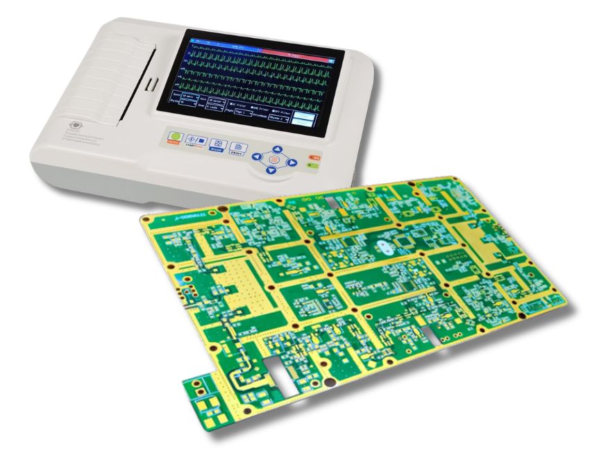
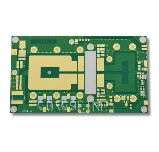
We produce precision high-frequency PCBs designed for high-frequency medical equipment. Our advanced manufacturing capabilities and certified quality standards deliver stable signal performance, tight tolerances, and maximum reliability above 500 MHz.

• ISO 13485, ISO 9001 & IPC-A-610 Class 2/3 Compliant
• Extensive In-Stock RF Laminates Including Rogers, Taconic, Arlon & PTFE-Based Materials
• Advanced Micro-Via Capabilities with 4mil Laser Drilling & Ultra-Fine Lines

Medical High-Frequency PCB
Certifications
What is Medical High-Frequency PCB
introduction

What is Medical High-Frequency PCB?

A medical high-frequency PCB is engineered to operate at high frequencies with minimal signal loss and ultra-low distortion. By utilizing specialized low-loss substrate materials, precise impedance control, and advanced layer stackups, we build high-speed circuit boards that maintain stable electrical performance in critical healthcare environments. This high-frequency construction is essential for modern medical devices, delivering the rapid data transmission, noise immunity, and uncompromised precision required for MRI systems, medical radar, wireless patient monitoring, surgical tools, and life-critical diagnostic equipment.

Products

Advantages of Medical High-Frequency PCB

  • Superior Signal Integrity
  • Stable Dielectric Constant (Dk)
  • Wide Frequency Range Support
  • Environmental Stability & Moisture Resistance
  • Tight Controlled Impedance
Superior Signal Integrity
Low-loss materials such as PTFE and ceramics reduce signal loss, distortion, and attenuation. This helps medical devices maintain accurate and stable signals during high-speed data transmission.
Stable Dielectric Constant (Dk)
Wide Frequency Range Support
Environmental Stability & Moisture Resistance
Tight Controlled Impedance
Why Choose Us

MedPCB as Medical High-Frequency PCB Manufacturer

  • ISO 13485 Certified Manufacturing

    ISO 13485 Certified & High-Frequency Materials

    MedPCB operates under ISO 13485 quality management standards for medical PCB manufacturing. We support high-frequency materials such as Rogers, PTFE, ceramics, and other low-loss laminates for medical imaging, monitoring, and high-speed medical electronics.

  • Precision Impedance Control & Signal Integrity

    Precision Impedance Control & Signal Integrity

    We control trace width, dielectric thickness, copper thickness, and layer spacing to meet your target impedance. For high-speed and RF designs, we combine impedance testing with design analysis and probing to help control signal loss, crosstalk, reflections, and phase instability.

  • Fine Trace Width Manufacturing

    Fine Trace Width Manufacturing

    Our fine-line PCB manufacturing capabilities support high impedance targets and dense medical layouts. Narrow, controlled traces help achieve accurate impedance matching while reducing signal dispersion. This is especially important for high-frequency and mmWave applications above 30 GHz.

  • Backdrilled & Filled Via Support

    Backdrilled & Filled Via Support

    We support backdrilled vias to remove unwanted via stubs that can cause signal reflections and insertion loss. For dense BGA and HDI layouts, filled vias can reduce impedance discontinuities and provide more reliable signal paths in compact medical devices.

  • High-Performance Substrate Selection

    Hybrid High-Frequency Stackups

    To help control PCB cost, we can build hybrid stackups that combine high-frequency laminates with standard FR-4. RF signals can be routed through dedicated high-frequency layers while FR-4 supports the remaining layers. This approach can reduce material costs while maintaining the electrical performance required for critical medical circuits.

Specs

Technical Specifications

Technical Parameter

Advanced High-Frequency Capability

HF Materials

Rogers RO4000/3000, Taconic TLY/RF, Megtron 6, Arlon, Isola Astra

Layer Count

Up to 40 layers for complex RF and high-speed designs

Dielectric Thickness

Down to 0.05 mm (2 mil) for thin, high-speed stack-ups

Impedance Control

±5% controlled impedance

Minimum Trace / Spacing

0.05 / 0.05 mm (2 / 2 mil) for dense RF routing

Microvias

0.1 mm laser-drilled microvias with stacked, staggered, and any-layer HDI

Via Filling

Resin- or copper-filled and capped via-in-pad

Via Aspect Ratio

Up to 12:1 for reliable deep-via plating

Surface Finishes

ENEPIG, Immersion Silver, and Immersion Tin

Heavy Copper

Up to 100 oz for high-power and thermal applications

Registration Accuracy

±0.05 mm (2 mil) for accurate layer registration

Technical Specifications
Capabilities

MedPCB Medical High-Frequency PCB Process

Step 1. DFM Review and Stack-Up Design

We review the Gerber files, layer stack-up, impedance requirements, and operating frequency. The design is checked for controlled impedance, dielectric thickness, trace geometry, and signal isolation. We also verify material compatibility before production.

Step 2. High-Frequency Material Preparation
Step 3. Precision Fabrication and Lamination
Step 4. Drilling, Plating, and Surface Finishing
Step 5. Electrical Testing and Quality Inspection
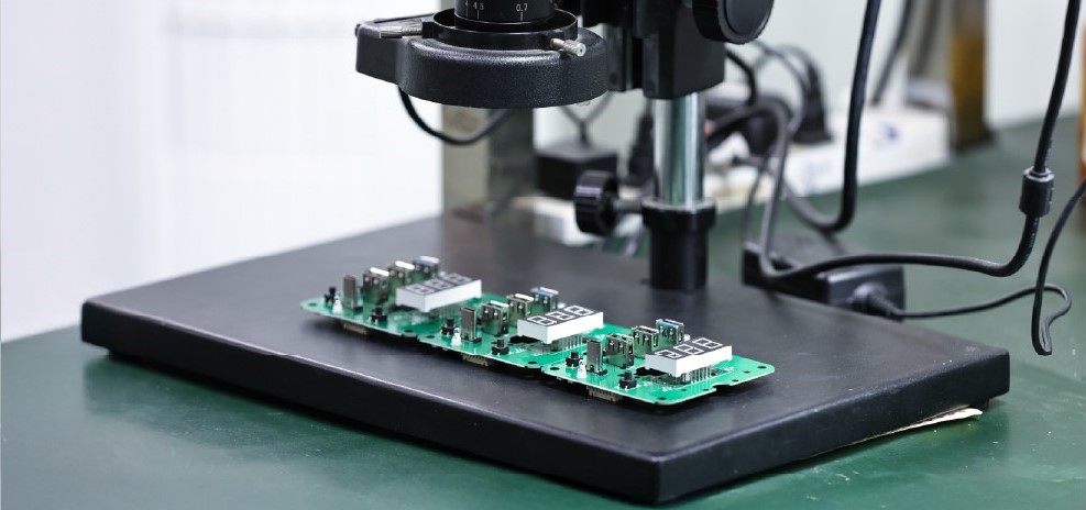
Each finished board undergoes dimensional, visual, and electrical inspection. Depending on the application, testing may include impedance testing, continuity testing, insulation resistance testing, and high-frequency performance verification. Final inspection confirms compliance with the specified drawings, tolerances, and quality standards.

Quality Control

Common Challenges in Medical High-Frequency PCB Manufacturing

  • Controlled Impedance Consistency

    Controlled Impedance Consistency

    Challenge: Small changes in trace width, etching, or dielectric thickness can affect impedance. This may cause signal loss, reflections, and data errors in high-frequency medical devices.

    Our Solution: We use precision imaging, controlled etching, and impedance testing to maintain consistent high-frequency signal paths. Our engineering team reviews stack-up and impedance requirements during DFM.

  • Layer Registration & Lamination Accuracy

    Layer Registration & Lamination Accuracy

    Challenge: PTFE and ceramic materials have different flow characteristics during lamination. Poor control can lead to layer shifting, misregistration, voids, and inner-layer trace misalignment.

    Our Solution: MedPCB supports multilayer high-frequency PCB fabrication with precise layer registration and controlled lamination processes. Our manufacturing team controls stack-up construction and layer alignment to maintain reliable electrical and mechanical performance.

  • Moisture Control & Material Handling

    Moisture Control & Material Handling

    Challenge: RF and microwave laminates can absorb moisture during storage and production. Moisture can change dielectric properties, affect signal stability, and increase the risk of delamination during assembly or sterilization.

    Our Solution: We store high-frequency materials in climate-controlled areas and use controlled vacuum-baking processes before lamination. This helps keep materials dry and maintain stable electrical performance.

  • RF Testing & Process Verification

    RF Testing & Process Verification

    Challenge: Standard PCB tests may not detect signal loss, phase shifts, or impedance problems at gigahertz frequencies.

    Our Solution: MedPCB uses impedance testers and advanced inspection equipment to verify high-frequency PCB quality. For demanding RF designs, our engineering team reviews controlled impedance requirements during DFM and production. 

High-Frequency Materials Supported by PCBMay
Specs

High-Frequency Materials Supported by MedPCB

MedPCB maintains an extensive inventory of high-frequency laminates.

PTFE-Based Materials - PTFE laminates offer very low dielectric loss, low and stable Dk, and excellent high-frequency signal performance. They are well suited for RF and microwave circuits where signal integrity is critical. Our stocked PTFE-based materials include:
Rogers RT/duroid 5880
• Rogers RO3003
• Shengyi mmWave77
• Taconic TLY Series

Non-PTFE Materials - Non-PTFE laminates provide low signal loss, good thermal stability, reliable mechanical strength, and easier PCB processing. They are a practical choice for high-speed and high-frequency medical systems that also require consistent manufacturing. Our stocked non-PTFE materials include:
• Rogers RO4003C
• Rogers RO4350B
• Panasonic Megtron 6
• Isola Astra MT77

MedPCB supports high-frequency medical PCB manufacturing with specialized materials, controlled impedance, DFM review, and IPC Class 2/3 production. Send us your Gerber files for a material and manufacturing review.

Case Study

Medical Heavy Copper PCB Cases

  • Laser Scalpel 
    Laser Scalpel PCB Laser Scalpel 

    Laser Scalpel 

    High-frequency PCB designed for precise laser control and stable power delivery, supporting accurate energy output and reliable performance during surgical procedures.

  • Ultrasound Transducer Probe
    Ultrasound Transducer Probe PCB Ultrasound Transducer Probe

    Ultrasound Transducer Probe

    Compact high-frequency PCB designed for fast signal transmission between the transducer and imaging system, supporting clear, high-resolution ultrasound images.

  • Electrocardiogram (ECG)  
    Electrocardiogram (ECG)  PCB Electrocardiogram (ECG)

    Electrocardiogram (ECG)  

    Low-noise medical PCB designed for precise cardiac signal acquisition, with effective filtering and signal isolation for accurate real-time heart monitoring.

  • Microwave Therapy Equipment 
    Microwave Therapy Equipment PCB Microwave Therapy Equipment 

    Microwave Therapy Equipment 

    High-frequency PCB designed for stable microwave signal generation and controlled energy delivery, supporting consistent treatment output and reliable operation during medical procedures.

Faqs

Frequently Asked Questions

Our Medical High-Frequency PCB FAQ addresses essential questions regarding your manufacturing requirements. We cover our capabilities for complex medical electronics, supply chain management, assembly timelines, rigorous quality inspection protocols, and our capacity to scale from initial builds to production batches. For every medical device project, we guarantee precision-focused, medical-grade assembly standards.

1. What Are The Key Characteristics Of High-Frequency PCBs?
Key features include low signal loss, controlled impedance, stable materials, and reliable high-speed signal transmission.
2. Do You Support Controlled Impedance PCB Manufacturing?
Yes. PCBMay supports controlled impedance PCB manufacturing and can review your stack-up, trace geometry, and material selection during DFM. Impedance testing helps verify that the finished board meets the required specifications.
3. Can You Manufacture Hybrid FR-4 and RF PCB Stackups?
Yes. PCBMay supports hybrid stack-ups that combine standard FR-4 with high-frequency materials. This approach can reduce material costs while keeping critical RF signals on low-loss dielectric layers.
4. What Materials Are Commonly Used In High-Frequency PCBs?
Common materials include PTFE, ceramic-filled laminates, and Rogers materials. These provide low dielectric loss and stable performance at high frequencies.
5. What Should I Look For When Choosing High-Frequency Materials?
Choose materials with low Dk, low Df, strong thermal stability, and low moisture absorption for consistent high-frequency performance.
6. How Do High-Frequency PCBs Differ From Standard PCBs?
High-frequency PCBs use specialized low-loss materials for signals above 1 GHz. Standard FR-4 may have higher signal loss at these frequencies.
7. Does Moisture Absorption Affect High-Frequency Materials?
Yes. Moisture can change the material’s electrical properties and affect signal stability. Low-moisture materials provide more consistent performance.

Product Related