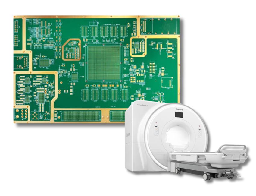
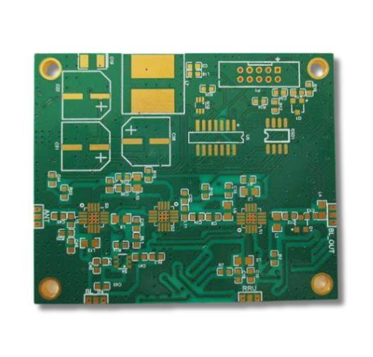
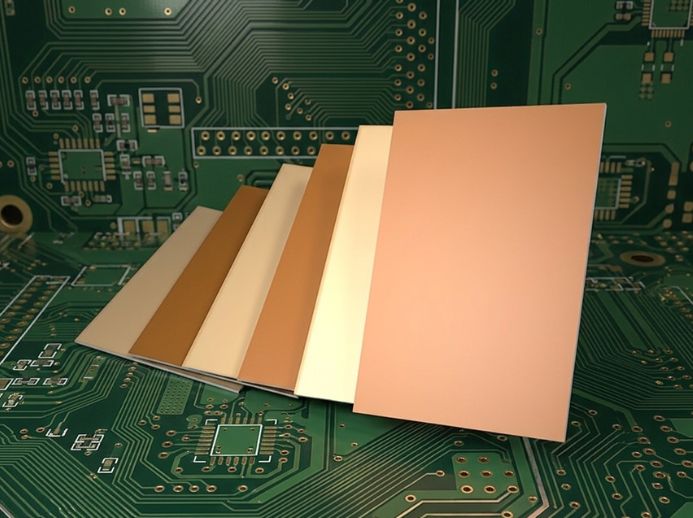
Panasonic MEGTRON 6 is a high-speed PCB material developed by Panasonic for medical electronics that require low signal loss, high thermal resistance, and stable electrical performance. Its low dielectric constant and ultra-low loss properties support reliable high-frequency signal transmission with strong signal integrity. MEGTRON 6 also supports high-density interconnect (HDI) PCB designs and maintains stable electrical performance under demanding thermal conditions. This makes Panasonic MEGTRON 6 suitable for high-speed medical equipment where signal integrity, heat resistance, and long-term PCB reliability are critical.
|
Capability |
Specification |
|
Layer
Count |
1–40 layers |
|
Megtron
Materials |
Standard Megtron 6 (R-5775 / R-5670) Halogen-Free Megtron 6 (R-5375 / R-5370) |
|
PCB
Types |
HDI, high-layer-count, blind/buried via,
heavy copper, and backdrill |
|
Board
Thickness |
0.2–5.0 mm |
|
Copper
Thickness |
0.5–10 oz |
|
PTH
Wall |
25 μm (1 mil) |
|
Maximum
Board Size |
1100 × 500 mm |
|
Min.
Laser Drill |
4 mil |
|
Min.
Trace / Spacing |
2.7 / 2.7 mil |
|
Solder
Mask Colors |
Green, black, blue, red, white, yellow,
purple |
|
Surface
Finishes |
ENIG, ENEPIG, HASL, Lead-Free HASL, OSP,
Immersion Silver, Immersion Tin, and Gold Plating |
|
Min.
Annular Ring |
3 mil |
|
Aspect
Ratio |
Up to 10:1 |
|
Impedance
Control |
±5 Ω (<50 Ω); ±10% (≥50 Ω) |
|
Additional
Technologies |
Blind/buried vias, via-in-pad, gold fingers,
press-fit, backdrill, electrical testing |


Challenge: Asymmetrical multilayer stackups can increase board warpage and mechanical stress, while affecting impedance consistency in high-speed designs.
Our Solution: We perform thorough DFM checks to maintain balanced and symmetrical layer distribution. This helps reduce board warpage and mechanical stress while keeping impedance more consistent for reliable performance.

Challenge: Minute variations in dielectric thickness or trace width disrupt signal integrity, causing high-speed data loss or signal noise in critical patient care systems.
Our Solution: We maintain ultra-tight manufacturing tolerances on Megtron 6 dielectric layers, guaranteeing strict controlled impedance of ±5 Ω (<50 Ω); ±10% (≥50 Ω)

Challenge: High-density MEGTRON 6 designs require tight control of lamination, drilling, and registration to maintain reliable interconnections.
Our Solution: We utilize specialized laser drilling parameters, optimized tool feeds, and controlled vacuum lamination profiles to prevent voids and achieve clean microvia geometry without fiber damage.

Challenge: High global demand for Megtron 6 can cause material shortages, resulting in costly production delays for time-sensitive medical device projects.
Our Solution: We maintain a strategic safety stock of core Megtron 6 laminates while stocking qualified high-frequency alternatives like Rogers RO4350B, Shengyi, and Isola I-Speed to keep your build on schedule.

The following specifications are based on Panasonic Industry's MEGTRON 6 R-5775(N)/R-5670(N) materials:
|
Property |
R-5775(N)/R-5670(N) |
|
Tg (DSC) |
185°C |
|
Tg (DMA) |
210°C |
|
Td |
410°C |
|
Dk @ 1 GHz |
3.4 |
|
Df @ 1 GHz |
0.002 |
|
CTE-Z < Tg |
45 ppm/°C |
|
Water Absorption |
0.14% |
|
Flammability |
UL 94V-0 |
MedPCB supports your medical MEGTRON 6 PCB projects with expert material selection, free DFM review, and IPC Class 2/3 manufacturing. Contact our engineering team today to discuss your requirements and get a tailored PCB solution.
Our Medical MEGTRON 6 PCB FAQ addresses essential questions regarding your eco-friendly manufacturing requirements. We cover our capabilities for multilayer halogen-free circuits, material selection, thermal stability, strict ISO 13485 quality standards, and compliance with RoHS and REACH regulations. For every medical PCB project, we guarantee high-precision fabrication tailored for critical healthcare applications.
English
French
German
Japanese
Korean