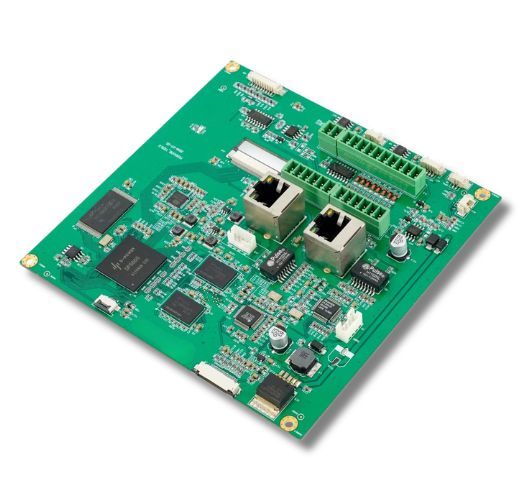
Ultrasound Equipment PCB

Ultrasound equipment PCBs support high-speed signal processing, imaging, and control circuits. These boards require stable signal transmission, precise impedance control, and reliable multilayer construction. MedPCB manufactures and assembles HDI and multilayer PCBs for ultrasound systems using high-frequency laminates and other suitable medical-grade materials.

✔ HDI and multilayer PCB manufacturing for compact ultrasound systems 
✔ High-frequency laminates and materials available 
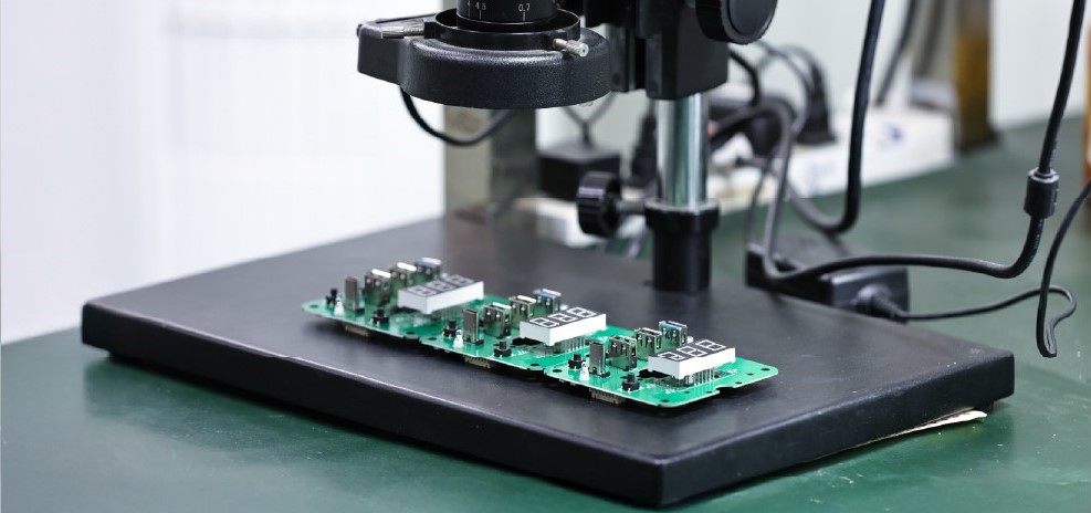
✔ 100% electrical testing, AOI, 3D X-Ray, and functional testing  
✔ ISO 13485 & IPC Class 2/3 PCB Manufacturing & Assembly

Ultrasound Equipment PCB
Certifications
What is Ultrasound Equipment PCB
introduction

What is Ultrasound Equipment PCB?

An ultrasound equipment PCB is a specialized circuit board used inside ultrasound machines. It controls key electronic functions, including signal transmission, echo reception, image processing, and system control.

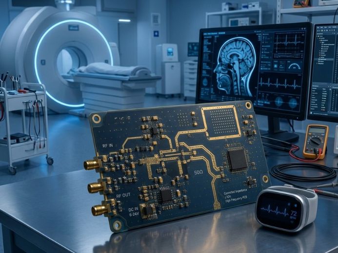
Ultrasound PCBs must provide stable signal transmission and reliable electrical performance. High-speed signals can be sensitive to noise and signal loss. For this reason, the PCB may require controlled impedance, multilayer construction, HDI technology, and suitable high-frequency materials.

The PCB works with the ultrasound transducer to process electrical signals into diagnostic images. Its design and manufacturing quality can affect signal integrity, imaging performance, and overall system reliability.

MedPCB manufactures and assembles ultrasound equipment PCBs for medical imaging systems. We support HDI, multilayer, rigid, and high-frequency PCB designs for prototypes, low-volume production, and volume manufacturing. Our medical PCB manufacturing and assembly follows ISO 13485 and IPC Class 2/3 requirements.

Quality

Features of Ultrasound Equipment PCB 

  • High Signal Integrity
  • Low-Noise Receive
  • Signal Processing & Beamforming
  • High-Voltage Transmit
High Signal Integrity
Ultrasound PCBs must maintain signal quality between the transducer and imaging circuits. Controlled impedance and accurate routing help reduce signal loss and interference, supporting clear and consistent diagnostic images.
Low-Noise Receive
Signal Processing & Beamforming
Ultrasound PCBs support signal processing and beamforming across multiple transducer channels. High-density multilayer and HDI designs help manage complex connections and maintain consistent signal timing for reliable medical imaging.
High-Voltage Transmit
Ultrasound transmit circuits may generate high-voltage pulses to excite transducer elements. PCB layout and assembly must provide appropriate creepage, clearance, insulation, and component spacing for the required operating conditions.
Why Choose Us

MedPCB as Ultrasound Equipment PCB Partner

  • ISO 13485 Certified Halogen-Free PCB Production

    ISO 13485-Certified Medical PCB Manufacturing & Assembly

    MedPCB manufactures and assembles medical PCBs under an ISO 13485-certified quality system. We support prototype and volume production with strict process control, traceability, and inspection for ultrasound equipment.

  • High-Frequency PCB Manufacturing for Ultrasound Equipment

    High-Frequency PCB Manufacturing for Ultrasound Equipment

    We manufacture high-frequency PCBs for ultrasound transmit, receive, and signal processing circuits. Controlled impedance, multilayer fabrication, and precise routing help maintain signal quality in medical imaging systems.

  • Turnkey PCB Assembly & Component Sourcing

    Turnkey PCB Assembly & Component Sourcing

    MedPCB provides turnkey PCB assembly, from component sourcing and SMT placement to soldering, inspection, and final testing. This helps simplify production and keeps the entire PCBA process under one supplier.

  • Free DFM/DFA Check for Ultrasound Equipment PCBs

    Free DFM/DFA Check for Ultrasound Equipment PCBs

    Our engineers provide a free DFM/DFA check before production. We review component placement, trace spacing, pad design, drilling, assembly clearances, and other details to help prevent manufacturing issues and identify manufacturing and assembly risks before production.

Specs

Technical Specifications
Technical Parameter

Manufacturing Capability

Order Quantity

≥ 1 PCS

Quality Grade

IPC-6012 Class 2 & Class 3

Board Size

Standard: up to 500 × 600 mm; Advanced: up to 1100 × 500 mm

Layer Count

1–40 layers. Supports multilayer and hybrid stackups for ultrasound equipment

Assembly Technologies

Surface Mount (SMT), Through-Hole (THT/DIP), and Mixed-Technology

Component Sourcing

Full Turnkey, Partial Turnkey, or Consigned (access to 300,000+ genuine parts)

Component Range

From 01005 packages to 0.2 mm fine-pitch BGAs (no maximum component size limit)

Placement Accuracy

±0.035 mm via automated component placement

Board Thickness

0.2–10.0 mm. Standard: 0.2–3.2 mm; Advanced: 3.4–10.0 mm

Copper Thickness

17–350 μm (0.5–10 oz). Standard: 0.5–4 oz

Min. Trace Width / Spacing

Internal: 3/3 mil (0.075 mm); External: 3/3 mil advanced, 3.5/4 mil standard, depending on copper weight

Surface Finish

ENIG, ENEPIG, Lead-Free HASL, OSP, Immersion Silver, Immersion Tin, Flash Gold, Hard Gold, Soft Gold, and combination finishes

Impedance Tolerance

±5 Ω for <50 Ω; ±10% for ≥50 Ω

Materials

FR-4, high-Tg materials, high-frequency laminates, and other materials suitable for ultrasound applications

Get Instant Quote
Technical Specifications Ultrasound Equipment PCB
How to choose

Ultrasound Equipment PCB Assembly Process

Step 1: Engineering Review & DFM/DFA
We review your ultrasound PCB design, component placement, and assembly requirements. The engineering team checks pad design, spacing, component clearance, and other details to help prevent manufacturing and assembly issues.
Step 2: PCB Fabrication & Component Sourcing
Step 3: IQC Incoming Quality Check
All incoming PCBs and components go through IQC before assembly. We check part numbers, quantities, specifications, and material condition to verify that the materials meet your requirements.
Step 4: SMT & THT Assembly
We assemble ultrasound equipment PCBs using automated SMT and THT processes. Solder paste printing, component placement, soldering, and through-hole assembly are controlled to ensure consistent assembly quality.
Step 5: Inspection, Functional Testing & Lot Traceability
Finished PCBAs may undergo SPI, AOI, X-ray inspection, electrical testing, and functional testing according to the component packages, assembly requirements, and approved test plan. Production records and lot traceability are maintained to support quality control and medical device manufacturing requirements.
challenges

Challenges in Ultrasound Equipment PCB Manufacturing and Assembly

  • High-Voltage Assembly

    High-Voltage Assembly

    Challenge - Ultrasound transmit circuits can generate high-voltage pulses that require proper PCB spacing and insulation. Poor clearance or assembly control can increase the risk of electrical failure.

    Our Solution - We review creepage, clearance, component spacing, and soldering requirements during DFM/DFA. Controlled assembly processes help maintain the required electrical clearances, insulation, and soldering quality.

  • Low-Noise Analog & Mixed-Signal Assembly

    Low-Noise Analog & Mixed-Signal Assembly

    Challenge - Ultrasound receive circuits handle weak signals and can be sensitive to electrical noise. Poor grounding, component placement, or soldering can affect signal quality.

    Our Solution - We review component placement, grounding, signal routing, and mixed-signal areas before assembly. Precise SMT placement and controlled soldering help maintain stable signal performance.

  • Fine-Pitch & High-Density Assembly

    Fine-Pitch & High-Density Assembly

    Challenge - Ultrasound systems often contain many channels and components in a compact space. Fine-pitch packages and dense layouts require accurate component placement and soldering.

    Our Solution - We support fine-pitch SMT assembly and high-density PCB designs. SPI, AOI, 

  • Component Sourcing & Supply Continuity

    Component Sourcing & Supply Continuity

    Challenge - Medical ultrasound PCBs may use specialized ICs, sensors, connectors, and other components. Component shortages or substitutions can affect production and product consistency.

    Our Solution - We source components through qualified suppliers and verify part numbers and specifications through IQC. Approved alternatives can also be reviewed when required to help maintain production continuity.

MedPCB Supported Technologies for Ultrasound PCB & PCBA Projects
Specs

MedPCB Supported Technologies for Ultrasound PCB & PCBA Projects

HDI PCB
We manufacture HDI PCBs for compact high-density ultrasound electronics. Our HDI process features fine-line routing and microvias for space-limited designs.

High-Frequency & Low-Loss PCB
We fabricate low-loss PCBs using Rogers, Taconic and similar laminates. Controlled impedance and tight tolerances ensure stable signal transmission for ultrasound circuits.

Rigid-Flex PCB
MedPCB provides rigid-flex PCB manufacturing for ultrasound devices that need flexible connections within compact mechanical assemblies. We control bend areas, layer registration, copper routing, and flex-to-rigid transitions to support reliable connections in handheld probes and space-constrained equipment.

Mixed-Technology PCBA
We perform mixed SMT and through-hole assembly for ultrasound PCBAs with full process quality control. Our production supports BGA, QFN, LGA, and other small-pitch packages, with solder paste inspection, AOI, X-ray inspection, and controlled reflow profiles for reliable solder joints.

MedPCB delivers one‑stop PCB fabrication and assembly services. Send us your inquiry for your ultrasound PCB & PCBA project.

Case Study

Ultrasound Equipment PCB Case Studies

  • Cart-Based Ultrasound PCB
    Cart-Based Ultrasound PCB Cart-Based Ultrasound

    Cart-Based Ultrasound

    The customer required a high-density PCB for multi-channel signal processing and system control. MedPCB manufactured an 8-layer rigid-flex PCB with microvias, fine-line routing, and controlled impedance to support high channel counts in a compact structure. The PCBA used fine-pitch SMT components and underwent SPI, AOI, X-ray, and functional testing before delivery. 

  • Echocardiography 
    Echocardiography PCB Echocardiography

    Echocardiography 

    The customer required a low‑loss PCB for real‑time Doppler signal acquisition. MedPCB produced a 10‑layer PCB using Rogers low‑loss laminate, with controlled dielectric thickness and impedance. The board was populated with BGA and fine‑pitch IC components. We performed X‑ray inspection on BGA solder joints to ensure reliable interconnection.

  • Endoscopic Ultrasound
    Endoscopic Ultrasound PCB Endoscopic Ultrasound

    Endoscopic Ultrasound 

    The project required a miniature and flexible PCB for integration into a compact ultrasound probe. MedPCB fabricated a 4-layer flex PCB with fine traces, microvias, and flexible polyimide construction for repeated bending. The PCBA used fine-pitch SMT components and passed dimensional, bend-reliability, soldering, and electrical continuity testing. 

  • Obstetrics & Gynecology Ultrasound 
    Obstetrics & Gynecology Ultrasound PCB Obstetrics & Gynecology Ultrasound

    Obstetrics & Gynecology Ultrasound 

    The customer needed low crosstalk PCBA for 4D high resolution multi channel imaging. MedPCB built a 10 layer Isola material PCB with optimized ground plane shielding and tight layer registration. We sourced 300+ components and performed SMT & selective THT mixed assembly with ±0.035 mm placement accuracy.

  • 2D_3D Ultrasound Systems
    2D_3D Ultrasound Systems PCB 2D_3D Ultrasound Systems

    2D/3D Ultrasound Systems

    The customer needed high-bandwidth routing for image processing and data acquisition circuits. MedPCB manufactured a 12-layer multilayer PCB with Panasonic Megtron 6 with high-density routing. The PCBA was assembled using automated SMT processes and passed SPI, AOI, impedance, electrical continuity, and functional testing. 

Faqs

Frequently Asked Questions

Our Ultrasound Equipment PCB FAQ addresses essential questions regarding your eco-friendly manufacturing requirements. We cover our capabilities for multilayer halogen-free circuits, material selection, thermal stability, strict ISO 13485 quality standards, and compliance with RoHS and REACH regulations. For every medical PCB project, we guarantee high-precision fabrication tailored for critical healthcare applications.

1. Do You Provide Full PCBA Assembly Service for Ultrasound PCBs?
Yes. MedPCB provides complete PCB and PCBA manufacturing, including PCB fabrication, component sourcing, SMT and THT assembly, inspection, and functional testing. We can also support fine-pitch, BGA, HDI, and high-density ultrasound PCB assemblies.
2. What's The Typical Lead Time For A Portable Ultrasound Prototype Build?
Our typical quick-turn prototype lead time for PCB fabrication and assembly always depends on layer count, material availability, and HDI complexity. Contact us directly at sales@medicalpcb.com
3. Why Do Ultrasound PCBs Require Rogers High-Frequency Materials?
Ultrasound systems process high-frequency signals with minimal loss. Rogers PCB laminates offer low dielectric loss (Df), stable dielectric constants (Dk), and superior thermal performance, preventing signal degradation and ensuring precise transducer wave management.
4. What Is The Typical Layer Count For Ultrasound PCBs?
Ultrasound PCBs typically range from 8 to 24+ layers, depending on system complexity. High layer counts are required to accommodate high-density interconnect (HDI) microvias, dedicated ground and power planes, and complex routing for multi-channel transducers.
5. Is IPC Class 2 Acceptable For Ultrasound PCBs?
While IPC Class 2 may be used for non-critical or commercial-grade equipment, medical-grade ultrasound devices generally require IPC Class 3. Class 3 standards guarantee continuous high performance, stringent quality control, and zero downtime for life-critical diagnostic systems.
6. Can You Handle Transitions From Prototype To Mass Production?

Yes, MedPCB supports the full product lifecycle, transitioning seamlessly from initial rapid prototyping and New Product Introduction (NPI) to scalable high-volume production with consistent quality and optimized costs.

Product Related