Medical HDI PCB

MedPCB provides precision High-Density Interconnect (HDI) PCB manufacturing and assembly for medical devices, combining ISO 13485-certified quality controls with microvia technology for ultra-compact, high-reliability electronics.

• ISO 13485, ISO 9001 & IPC-A-610 Class 2/3 Compliant.
• Up to 40-Layer HDI PCB Fabrication
• Supports 1+N+1, 2+N+2, and Any-Layer HDI structures.
• Microvias, fine lines, and sequential lamination capabilities.
• Blind, buried, stacked, and staggered via configurations.

Medical HDI PCB
Certifications
What is Medical HDI PCB
introduction

What is Medical HDI PCB?

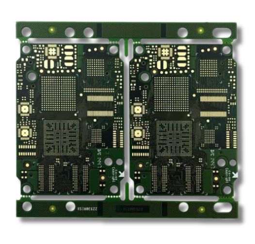
A medical HDI PCB (High-Density Interconnect) uses advanced manufacturing techniques like microvias, fine-line routing, and sequential lamination to pack more wiring into a much smaller footprint. HDI technology increases routing density through laser-drilled microvias, fine-line routing, and sequential lamination, allowing more components and signal traces to fit within a smaller PCB area. This ultra-dense construction is essential for next-generation medical technology, enabling lightweight, highly compact designs without compromising the precision, signal integrity, and rock-solid reliability required for life-saving devices.

Products
 

Advantages of Medical HDI PCB

  • Compact, Space-Saving Design
  • Fine-Pitch Routing for High Component Density
  • Superior Signal Integrity
  • Flexible HDI Structures for Complex Medical Designs
  • Long-Term Cost-Effectiveness
Compact, Space-Saving Design
By placing ultra-narrow traces and microscopic microvias closer together, HDI technology packs maximum functionality into an exceptionally small footprint. This makes it ideal for lightweight wearables, portable diagnostic tools, and space-constrained medical devices.
Fine-Pitch Routing for High Component Density
Superior Signal Integrity
Flexible HDI Structures for Complex Medical Designs
Long-Term Cost-Effectiveness
While the initial manufacturing setup is precise, consolidating multiple standard boards into a single, highly integrated HDI board significantly cuts overall material costs, simplifies final assembly, and reduces long-term testing and maintenance expense.
Why Choose Us

Choosing MedPCB as Medical HDI PCB Partner

  • ISO 13485 Certified Medical Quality

    ISO 13485 Certified Medical Quality

    Our production operates strictly under ISO 13485 certified quality systems and IPC Class 3 standards. Combined with medical-grade materials from top suppliers, we ensure your medical HDI assemblies meet every global safety and regulatory requirement.

  • Advanced Microvia & Via-in-Pad Capabilities

    Advanced Microvia & Via-in-Pad Capabilities

    We offer precision Via-in-Pad and copper-filled microvias to eliminate complex BGA fan-out routing and maximize available board space. This ultra-dense interconnection technology allows for seamless placement of high-pin-count components in compact medical devices.

  • Flexible & Any-Layer HDI Stackups

    Flexible & Any-Layer HDI Stackups

    From standard 1+N+1 and 2+N+2 structures to complex stacked/staggered microvias and Any-Layer HDI, we support customized stackup configurations. Whatever your density requirements demand, we engineer stackups built for maximum performance and manufacturability.

  • Up to 40-Layer HDI Manufacturing

    Up to 40-Layer HDI Manufacturing

    We manufacture complex, ultra-dense HDI boards with up to 40 layers. This high layer-count capability allows us to handle the most demanding circuitry for next-generation medical equipment without increasing physical board size.

  • Controlled Impedance for High-Speed Medical Electronics

    Controlled Impedance for High-Speed Medical Electronics

    We deliver precise controlled impedance (down to ±5%) to protect signal stability in high-frequency medical circuits. By accurately managing trace geometry and dielectric spacing, we guarantee zero signal distortion for sensitive diagnostic and imaging electronics.

Specs

Technical Specification

Feature

Standard HDI PCB

Advanced HDI PCB

Layer Count

1–20 layers

22–40 layers

Blind & Buried Vias

Mechanical vias with up to 3 lamination cycles

Mechanical vias with up to 2 lamination cycles

HDI Stackup

1+N+1, 2+N+2, 3+N+3

1+N+1, 1+1+N+1+1, 2+N+2, 3+N+3

Laser Via Size

4–6 mil

4–6 mil

Microvia Technology

Laser blind vias with copper filling

Copper-filled laser blind vias and fine microvias

Minimum Trace / Space

0.075 mm / 0.075 mm

0.05 mm / 0.05 mm

Copper Weight

0.5–4 oz (18–140 μm)

0.3–100 oz

Board Thickness

0.2–3.2 mm

3.4–10.0 mm

Maximum Board Size

500 × 600 mm

1100 × 500 mm

Base Materials

FR-4, High-Tg FR-4, Rogers, PTFE, GETEK, Hybrid materials

Surface Finish

ENIG, OSP, Immersion Tin, Immersion Silver, Electrolytic Gold, Gold Fingers


Technical Specification HDI
Capabilities

MedPCB Medical HDI PCB Process

Step 1: Inner Layer Imaging & Etching
Circuit patterns are transferred onto an inner copper-clad core using Laser Direct Imaging (LDI) for exact trace accuracy. Unwanted copper is chemically etched away, and every layer undergoes Automated Optical Inspection (AOI) to eliminate defects before lamination.
Step 2: Sequential Lamination & Laser Microvia Drilling
Step 3: Metallization & Copper Via Filling
Step 4: Outer Trace Etching & Surface Finishing
Step 5: Electrical Testing & Quality Verification
Quality Control

Common Challenges in Medical HDI PCB Manufacturing

  • Microvia Reliability

    Microvia Reliability

    Challenge: Thermal cycling during operation or reflow can cause microvias especially stacked microvias, to crack, break, or delaminate, leading to intermittent signal failures in critical medical devices.

    Our Solution: MedPCB utilizes optimized copper plating and void-free copper filling to improve interconnection reliability and withstand repeated thermal cycling. Every microvia structure undergoes rigorous microsection analysis and thermal shock testing to ensure reliable IPC Class 3 interconnections.

  • Sequential Lamination Registration

    Sequential Lamination Registration

    Challenge: Multi-stage lamination cycles subject inner layers to high temperatures and pressures, causing material shrinkage and misregistration between ultra-fine microvia layers.

    Our Solution: We employ advanced X-ray target drilling and high-precision laser alignment systems to maintain exact layer-to-layer registration accuracy throughout sequential lamination cycles.

  • Fine-Line Etching Accuracy

    Fine-Line Etching Accuracy

    Challenge: Medical HDI PCBs feature ultra-dense layouts with tiny line widths and spaces (often less than 3 mil). Over-etching can break circuits, while under-etching causes short circuits, directly threatening device performance.

    Our Solution: MedPCB uses precision chemical etching equipment with real-time process monitoring. Our automated optical inspection (AOI) scans every panel to catch minute trace variations, guaranteeing sharp conductor profiles and flawless circuit continuity.

  • Controlled Impedance Consistency

    Controlled Impedance Consistency

    Challenge: Compact medical electronics rely on high-frequency signals. Trace width variations, layer thickness shifts, or dielectric irregularities disrupt signal integrity and degrade system accuracy.

    Our Solution: Our engineering team performs pre-production stack-up modeling to select optimal high-frequency laminates. We verify impedance values using Time-Domain Reflectometry (TDR) testing during production to guarantee strict signal integrity tolerances.

HDI Technologies Supported by PCBMay
Specs

HDI Technologies Supported by MedPCB

Laser-Drilled Microvias - Ultra-small interconnections between adjacent layers that enable maximum routing density for compact medical devices. Available as stacked microvias (copper-filled for high thermal cycling reliability) or staggered microvias to minimize mechanical stress across stack-ups.

Blind & Buried Vias - Eliminate full-thickness drill holes. Blind vias link outer signal layers to inner layers, while buried vias connect internal layers exclusively reserving surface real estate for high-density, fine-pitch component fan-out.

Via-in-Pad Technology - Resin-filled and copper-capped flat pads positioned directly under fine-pitch BGAs. This minimizes trace routing distance, enhances high-frequency signal integrity, and guarantees reliable solder joints.

Sequential Lamination - Multi-stage buildup processes that stack laser-drilled microvia layers onto a central core. Executed with strict registration control and resin flow management to ensure long-term thermal and mechanical stability under medical operating standards.

Need reliable medical HDI PCB manufacturing? Send us your Gerber files today for a quick quote!


Case Study

Medical HDI PCB Case Study

  • 3D Digital Breast Tomosynthesis 
    3D Digital Breast Tomosynthesis PCB 3D Digital Breast Tomosynthesis 

    3D Digital Breast Tomosynthesis 

    High-density interconnect (HDI) PCB built with microvias, fine traces, and controlled impedance to support high-speed image acquisition, low-noise signal transmission, and accurate 3D breast imaging.

  • Left Ventricular Assist Device 
    Left Ventricular Assist Device PCB Left Ventricular Assist Device 

    Left Ventricular Assist Device 

    Compact HDI PCB designed with stacked microvias, dense component placement, and reliable power distribution to deliver stable motor control and continuous operation in implantable cardiac devices.

  • Ambulatory Cardiac Patch
    Ambulatory Cardiac Patch PCB Ambulatory Cardiac Patch

    Ambulatory Cardiac Patch

    Ultra-compact HDI PCB featuring microvias and fine-line routing to support miniaturized electronics, low-power operation, and reliable wireless ECG monitoring in wearable medical devices.

  • Video Endoscopy Platform
    Video Endoscopy Platform PCB Video Endoscopy Platform

    Video Endoscopy Platform

    High-speed HDI PCB engineered with controlled impedance, laser-drilled microvias, and optimized signal integrity to deliver stable HD video transmission and real-time image processing in endoscopic systems.

Faqs

Frequently Asked Questions

Our Medical HDI PCB FAQ addresses essential questions regarding your manufacturing requirements. We cover our capabilities for complex medical electronics, supply chain management, assembly timelines, rigorous quality inspection protocols, and our capacity to scale from initial builds to production batches. For every medical device project, we guarantee precision-focused, medical-grade assembly standards.

1. What HDI Stackups Do You Support?
We support a full range of HDI stackup structures, including 1+N+1, 2+N+2, 3+N+3, and Any-Layer HDI (ELIC). We handle multi-stage sequential laminations with stacked, staggered, blind, and buried microvias, as well as via-in-pad setups tailored to your density requirements.
2. Can MedPCB Provide HDI PCB Assembly Services?
Yes. We provide complete turnkey HDI PCB assembly services. Our production lines are equipped with ultra-precise SMT placement machines capable of handling fine-pitch BGAs, 0201/01005 components, resin filling/capping, and 3D AOI/X-ray inspection for medical-grade reliability.
4. Are mSAP And Laser Drilling Necessary For All HDI?
No. Standard HDI with laser-drilled microvias covers most applications. Modified Semi-Additive Process (mSAP) is only needed for ultrafine traces (sub-50 µm line/space) found in compact devices, wearables, and advanced modules.
5. What Makes HDI PCBs Better Than Traditional PCBs?
HDI boards pack higher component density into a much smaller footprint. They offer superior signal integrity, better thermal management, and reliable performance for high-speed, compact electronics.
6. Why are HDI PCBs Harder To Manufacture?
They require specialized equipment such as precision laser drills for microvias along with sequential lamination and tight alignment tolerances, requiring higher precision than standard multi-layer boards.
7. Are Materials Other Than FR4 Used In Medical PCBs?
Yes. Medical electronics frequently use Polyimide (flexible/rigid-flex), PTFE/Teflon (high-frequency), or ceramic substrates to satisfy strict reliability, thermal, and mechanical demands.
8. Are HDI PCBs Worth The Higher Cost?
Yes, if your design demands extreme miniaturization or high performance. While harder to produce, HDI is essential for medical implants, diagnostics, smartphones, and 5G hardware.
9. What Lead Times Are Typical for HDI medical PCB?
Prototypes: 5–15 business days (depending on layer count and material availability) and Mass Production: 3–6 weeks (longer for exotic laminates or multi-step sequential lamination).
10. Can Small Batches Of Medical HDI PCB be Produced?
Yes. We fully support no-MOQ (Minimum Order Quantity) prototype runs to help you validate designs before full production.

Product Related