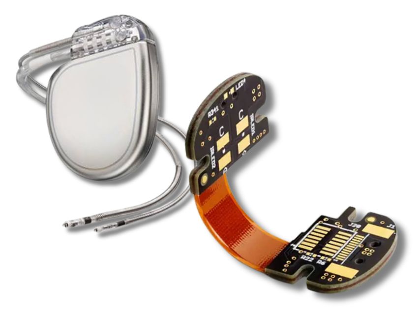
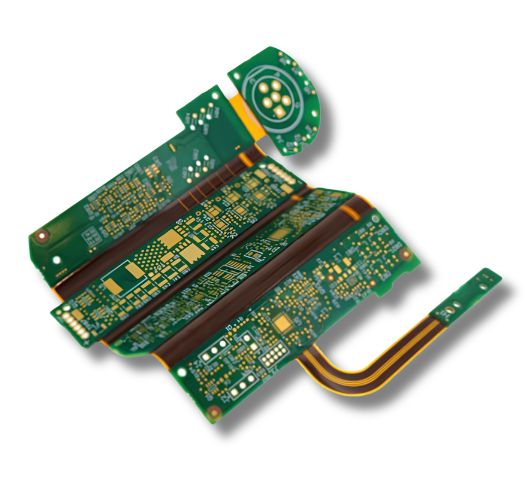
A medical rigid-flex PCB is a hybrid circuit board that combines the mechanical strength of traditional rigid boards with the bendable flexibility of flexible circuits. Designed to fit into compact spaces without sacrificing durability, these boards eliminate the need for wire harnesses, reducing weight and potential points of failure. They are widely used in medical wearables, surgical instruments, diagnostic imaging, and implantable devices that require high-density interconnects, long-term reliability, and space-saving designs.
Feature / Capability | Standard | Advanced |
Max Layers | 2–12 layers (up to 10 flex layers) | 13–20 layers (up to 18 flex layers) |
Min. Line Width / Spacing (Inner Layer, 12/18 µm Cu) | 3.5 / 3.5 mil (Partly 3.2 / 3.2 mil) | 3.0 / 3.0 mil (Partly 2.8 / 2.5 mil) |
Min. Line Width / Spacing (Outer Layer, 18 µm Cu) | 3.8 / 3.8 mil (Partly 3.2 / 3.5 mil) | 3.6 / 3.6 mil (Partly 3.0 / 3.3 mil) |
Min. Hole / Pad Size | Blind Via: 4 mil Max Buried Via: 0.4 mm | Blind Via: 4–6 mil Max Buried Via: 0.4 mm |
Rigid-Flex Board Thickness | 0.3 mm – 3.0 mm | 0.3 mm – 4.0 mm |
Max Copper Thickness | 2 oz | 3 oz |
Max Finished Copper Thickness | 3 oz | 5 oz |
Max Board Size | 406.4 mm × 558.8 mm | 406.4 mm × 736.6 mm |
Min. Board Size | 10 mm × 15 mm | 10 mm × 15 mm |
Supported Finishes | HASL, Lead-Free HASL, ENIG, ENEPIG, Electrolytic Nickel Gold, Soft Gold, Hard Gold, Immersion Silver, Immersion Tin, OSP | Same standalone finishes supported; Advanced combinations supported (ENIG+OSP, ENIG+Gold finger, Electrical Gold+Gold fingers) |

Production begins by selecting high-grade flexible polyimide substrates, rigid FR-4 cores, and copper foils tailored to the board's mechanical and bend requirements. Substrates undergo deep chemical cleaning to remove contaminants, ensuring pristine lamination bonding without voids. Common materials include:
• Adhesive FCCL: For standard flex layers.
• Adhesiveless FCCL: For thin, reliable designs.
• Coverlays & Adhesives: Protect and bond flex layers.
• PI Stiffeners: Reinforce connector and component areas.
• Rigid Cores: Provide heat resistance and stability.
• Low-Flow Prepregs: Join rigid and flex areas with less resin overflow.
Circuit patterns are transferred onto copper layers using high-resolution photolithography. Controlled chemical etching removes unwanted copper to define clean, fine-pitch traces. Plating and via metallization are then performed to build copper thickness across traces, plated through-holes, and microvias, establishing reliable electrical continuity across all layers.

Challenge: Transition zones where rigid FR-4 meets flexible polyimide are highly vulnerable to trace cracking, via fatigue, and delamination caused by bending and thermal expansion mismatches.
Our Solution: MedPCB integrates strain-relief fillets, overlapping coverlays, and no-flow prepregs along transition seams to distribute mechanical stress and safeguard trace integrity.

Challenge: Routing dense interconnections across rigid and flex regions creates severe mechanical stress points, increasing the risk of trace cracking and via failure.
Our Solution: We integrate high-density microvias alongside blind and buried via architectures contained strictly within the rigid sections. This maintains maximum wiring density while keeping flexible regions free of stress-prone hole penetrations.

Challenge: Ultra-thin flexible polyimide stretches and warps during etching and thermal reflow, leading to severe layer misregistration and component placement errors.
Our Solution: We secure flex layers using custom vacuum carrier jigs and laser-aligned tooling throughout production, keeping substrates flat and maintaining tight dimensional tolerances.

Challenge: Softer flexible materials tear or smear during mechanical drilling, creating copper burrs and poor hole-wall plating that compromise electrical connectivity.
Our Solution: We employ high-precision UV laser drilling for microvias down to 4 mil, paired with plasma desmear processing to guarantee flawless hole-wall plating and via reliability.

MedPCB supports multiple rigid-flex PCB structures to meet different routing density, bending radius, layer count, and packaging requirements for medical devices.
Traditional Rigid-Flex – This standard structure combines rigid and flexible layers in one PCB. It works well for medical devices that need simple routing, moderate component density, and reliable flex connections.
Asymmetrical Rigid-Flex – An asymmetrical stack-up uses different layer structures on each side of the flex section. This gives you more design freedom when the device has uneven space, component placement, or routing requirements.
Blind/Buried Via Rigid-Flex – Blind and buried vias connect selected layers without passing through the entire board. This saves routing space and keeps the design compact, making it suitable for medical devices with dense circuitry and limited board area.
HDI Rigid-Flex – HDI rigid-flex uses fine traces, microvias, and high-density routing to fit more circuits into smaller spaces. It is suitable for advanced medical electronics such as wearable monitors, imaging systems, surgical equipment, and portable diagnostic devices.
MedPCB supports rigid-flex structures based on your layer count, bend requirements, routing density, and device size. Our engineering team can review your design through a free DFM check for reliable medical PCB production.
Our Medical Rigid-Flex PCB FAQ addresses essential questions regarding your manufacturing requirements. We cover our capabilities for complex medical electronics, supply chain management, assembly timelines, rigorous quality inspection protocols, and our capacity to scale from initial builds to production batches. For every medical device project, we guarantee precision-focused, medical-grade assembly standards.
English
French
German
Japanese
Korean