1. How Can You Distinguish Between Single-Layer And Multilayer PCBs?
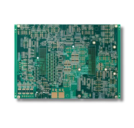
Single-layer PCBs have conductive copper on only one side of a single substrate. A multilayer PCB uses three or more copper layers. Insulating dielectric material separates the layers, while plated vias create electrical connections between them..
2. Why Are Multilayer PCBs Used In Medical Devices?
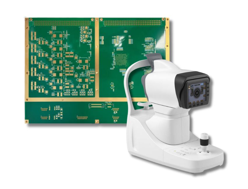
Multilayer PCBs allow us to build compact, high-density designs necessary for advanced medical electronics such as imaging systems, implants, and IoT-enabled diagnostic tools.
3. What Types Of Substrates Do You Use For Medical PCBs?
We offer a wide range of high-reliability substrates depending on your application, including standard high-Tg FR4, PTFE, Polyimide, and advanced laminates from industry leaders like Rogers, Isola, Arlon, and Nelco.
4. Why is EMC Required For Medical PCBs?
Electromagnetic Compatibility (EMC) is mandatory to ensure a medical PCB limits its own electromagnetic emissions. It prevents interference with nearby equipment while maintaining total immunity to external electromagnetic noise.
5. How Are Thermal Properties Managed In Complex Multilayer PCBs?
We utilize high-Tg dielectric materials, heavy copper layers, strategic thermal via arrays, and specialized heat sinks to rapidly dissipate thermal loads, preventing delamination and ensuring long-term electrical stability.
6. How Does Your Medical PCB Fabrication Process Maintain Signal Accuracy?
We ensure low signal loss through tight controlled impedance manufacturing, High-Density Interconnect (HDI) microvia technology, optimized layer stackups, and precise dielectric spacing across high-frequency circuits.
7. Can Medical PCBs Be Customized For Compact Wearable Devices?
Yes. We fabricate ultra-compact rigid-flex and flexible PCBs that fold into tight spaces. These lightweight, durable designs are engineered specifically for continuous health monitoring and portable medical wearables.
8. How Do You Ensure The Sterilization Compatibility Of Medical PCBs?
We utilize robust, high-temperature substrates and specialized conformal coatings that withstand harsh sterilization environments including autoclaving, chemical wipe-downs, and gamma radiation.
9. What Future Trends Are Shaping Medical Multilayer PCB Technology?
Advanced technologies are transforming medical multilayer PCBs to make healthcare devices smaller, faster, and more reliable:
• Advanced Materials & Thermal Management: Low-loss dielectrics and high-conductivity laminates enable high-frequency data streaming for real-time patient monitoring and high-power medical diagnostic equipment.
• HDI & Microvias: Sub-150-micron microvias allow extreme circuit miniaturization, paving the way for next-generation wearables, implantables, and compact surgical tools.
• Embedded Components: Placing passives directly inside inner board layers drastically shrinks device footprint while shortening signal paths for ultra-accurate vital sign readings.