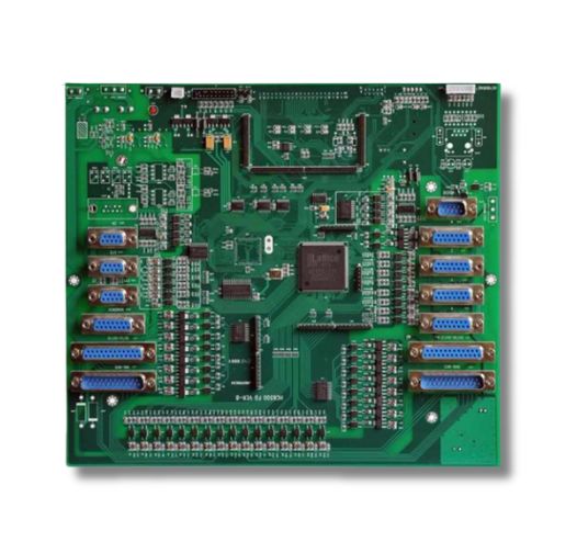
MRI Machine PCB

MedPCB manufactures and assembles MRI machine PCBs for RF, signal processing, control, and imaging electronics. We support non-magnetic material selection, high-frequency laminates, controlled impedance, multilayer and HDI PCB fabrication and assembly for MRI equipment.

✔ MRI-Compatible Material Selection Based on Project Requirements
✔ Controlled Impedance For High-Frequency MRI Signal Circuits
✔ Multilayer & HDI PCB Fabrication 
✔ Turnkey Component Sourcing & SMT/THT PCBA
✔ ISO 13485 & IPC Class 2/3 PCB & PCBA Manufacturing

MRI Machine PCB
Certifications
What is an MRI Machine PCB
introduction

What is an MRI Machine PCB?

An MRI machine PCB is a printed circuit board used in RF coils, signal processing, control, power, and imaging electronics within an MRI system.

MRI electronics operate in a highly controlled electromagnetic environment, where material selection, signal integrity, thermal performance, and mechanical reliability can all affect system performance. PCB materials and construction must therefore be selected according to the location and function of the board within the MRI system.

MedPCB manufactures and assembles MRI machine PCBs for prototypes, low-volume, and volume production. We support multilayer, HDI, rigid, and other PCB designs based on your MRI equipment requirements. Manufacturing and assembly follows ISO 13485 and IPC Class 2/3 quality requirements.

Quality

Important Properties of MRI Machine PCB

  • Thermal Conductivity for Heat Management
  • Dielectric Constant (Dk) for Signal Integrity
  • Low Dissipation Factor (Df) for Minimal Signal Loss
  • Low Electromagnetic Interference
Thermal Conductivity for Heat Management
MRI PCB substrates should provide suitable thermal conductivity for effective heat dissipation. This helps manage heat from components and RF circuits during continuous operation.
Dielectric Constant (Dk) for Signal Integrity
Low Dissipation Factor (Df) for Minimal Signal Loss
A low dissipation factor reduces dielectric signal loss at high frequencies. This helps preserve signal strength and supports accurate RF signal processing in MRI systems.
Low Electromagnetic Interference
MRI PCBs require materials that are suitable for strong magnetic field environments. Non-magnetic material selection helps reduce unwanted magnetic interference and supports reliable MRI system operation.
Why Choose Us

MedPCB as MRI Machine PCB Manufacturer

  • ISO 13485 Certified Halogen-Free PCB Production

    ISO 13485 & IPC Class 2/3  & PCBA Manufacturing

    MedPCB manufactures and assembles medical PCBs under an ISO 13485 quality management system and supports IPC Class 2 and Class 3 requirements. Production records, inspection controls, and material traceability are maintained according to project requirements.

  • MRI-Grade Substrate

    MRI-Grade Substrate

    We supply a wide range of high‑frequency, high‑speed and HDI‑grade PCB materials. Backed by robust supply‑chain resources, we deliver genuine, fully traceable substrates, including validated material grades built for MRI medical equipment.

  • Precision Multilayer & HDI Fabrication

    Precision Multilayer & HDI Fabrication

    Our manufacturing process supports multilayer, high-frequency, and complex MRI PCB designs using suitable non-magnetic materials and components. Controlled drilling, lamination, plating, and impedance fabrication help maintain the required electrical and mechanical performance while material selection helps reduce unwanted magnetic interference within MRI equipment.

  • Turnkey PCB Assembly & Component Sourcing

    Turnkey PCB Assembly & Component Sourcing

    MedPCB provides turnkey PCB assembly for MRI systems, covering component sourcing, SMT and through-hole assembly, soldering, inspection, and final testing. We can source approved components based on your BOM and maintain component traceability throughout production. Assembly processes are controlled to meet the reliability requirements of medical electronics.

  • Free DFM Check

    Free DFM Check

    Our engineering team reviews the PCB layout, stackup, trace spacing, drilling, materials, and other manufacturing requirements before production of your MRI machine PCB. This helps identify design issues early and reduce production risks.

  • Strict Inspection Quality

    Strict Inspection Quality

    Every MRI PCB undergoes electrical and visual inspection based on the approved quality requirements. Inspection can include 100% electrical testing (E-Test), AOI, 3D X-ray, and functional circuit testing (FCT) to verify PCB quality and assembly performance.

Specs

Technical Specifications

Technical Parameter

Manufacturing and Assembly Capability

Board Size

Standard: up to 500 × 600 mm

Advanced: up to 1100 × 500 mm

Layer Count

1–40 layers

Standard: 1–20 layers

Advanced: 22–40 layers, including hybrid stackups

Assembly Technologies

Surface Mount (SMT), Through-Hole (THT/DIP), and Mixed-Technology

Component Sourcing

Full Turnkey, Partial Turnkey, or Consigned (access to 300,000+ genuine parts)

Component Range

From 01005 packages to 0.2 mm fine-pitch BGAs (no maximum component size limit)

Placement Accuracy

±0.035 mm via automated component placement

Board Thickness

0.2–10.0 mm

Standard: 0.2–3.2 mm

Advanced: 3.4–10.0 mm

Min. Trace Width / Spacing

Internal: 3/3 mil (0.075 mm)External: 3/3 mil advanced; 3.5/4 mil standard, depending on copper weight

Surface Finish

ENIG, ENEPIG, Lead-Free HASL, OSP, Immersion Silver, Immersion Tin, Flash Gold, Hard Gold, Soft Gold, and combination finishes

Impedance Tolerance

±5 Ω for <50 Ω±10% for ≥50 Ω

PCB Materials

FR-4, High-Tg FR-4, Rogers, and other advanced materials based on MRI Machine design requirements

PCB Types

Multilayer, HDI, rigid, high-Tg, and hybrid PCB constructions

Technical Specifications MRI Machine
Capabilities

MRI Machine PCB Manufacturing and Assembly

Step 1. Engineering & DFM Review

We review the MRI PCB design, stackup, impedance requirements, layer count, trace spacing, vias, and material specifications. Our engineers check the design for manufacturing issues before fabrication.

Step 2. Material Selection & PCB Fabrication
Step 3. SMT & Through-Hole PCB Assembly
We verify the BOM and source approved components according to the your specifications. After material preparation, we conduct an IQC to SMT and THT components. Automated SMT equipment places surface-mount components, while through-hole components are assembled where required. Solder paste printing, component placement, and reflow soldering are controlled throughout the SMT process.
Step 4. PCBA Inspection & Testing
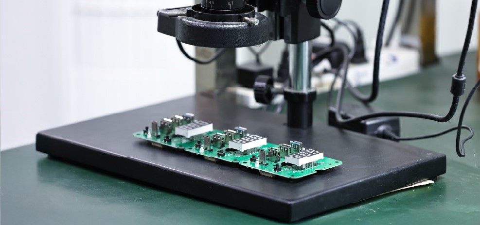
After assembly, PCBAs undergo in-process and final inspection according to the approved quality plan. SPI and AOI are used to monitor solder paste deposition, component placement, and visible soldering defects. X-ray inspection can be applied to BGAs, QFNs, and other components with hidden solder joints. ICT and functional circuit testing (FCT) are performed when required by the PCBA design and customer test specifications.
Step 5. Final Testing & Traceable Delivery
We complete final inspection, cleaning, labeling, and packaging before shipment. Production records, material information, inspection results, and component traceability are maintained according to the project's quality requirements.
challenges

Challenges in MRI Machine PCB Manufacturing & Assembly

  • RF and Mixed-Signal Assembly

    RF and Mixed-Signal Assembly

    Challenge: MRI systems combine RF, digital, analog, and power circuits on compact PCB assemblies. Poor component placement, soldering defects, or unwanted signal coupling can affect RF and mixed-signal performance.

    Our Solution: We use controlled SMT and through-hole assembly processes with precise component placement and solder paste inspection. SPI, AOI, 3D X-ray, and functional testing can be applied to verify solder joints, BGA connections, and critical components.

  • Thermal Management in High-Density Enclosures

    Thermal Management in High-Density Enclosures

    Challenge: MRI control and RF circuits can generate heat within compact enclosures. Poor heat dissipation can increase component stress and affect long-term PCB reliability.

    Our Solution: We consider thermal requirements during the PCB design and manufacturing review. Suitable copper weights, thermal vias, heat-spreading areas, and thermally stable materials can be used where required. We deploy tightly controlled reflow profiles to deliver consistent soldering quality for medical PCB assemblies.

  • Substrate Durability Under High-Frequency Loads

    Substrate Durability Under High-Frequency Loads

    Challenge: High-frequency MRI circuits place greater demands on PCB materials. Changes in dielectric properties, thermal stress, or material stability can affect signal performance over time.

    Our Solution: We provide quality PCB materials from approved and established suppliers. Material specifications are reviewed against the customer's requirements, while the final material selection follows the approved design and specifications. Selected Rogers, PTFE-based, and other high-frequency laminates can be supplied when specified for MRI and RF applications.

  • Long-Term Reliability & Manufacturing Quality

    Long-Term Reliability & Manufacturing Quality

    Challenge: MRI equipment is expected to operate reliably for many years. PCB failures can cause equipment downtime, maintenance costs, and replacement expenses.

    Our Solution: We use controlled manufacturing processes and inspection controls to reduce production defects. PCB electrical testing, impedance testing, AOI, X-ray inspection, ICT, and FCT can be applied 

 Technical Specifications MRI
Specs

MRI PCB & PCBA Testing Solutions

For your MRI electronics, MedPCB delivers reliable PCB fabrication and assembly services. We carry out multi‑dimensional testing on bare PCBs and completed PCBAs to verify electrical, mechanical and functional performance for your MRI equipment.

PCB Testing
• 100% E-Test — Checks electrical continuity and isolation.
• Impedance Testing — Verifies controlled impedance for RF and high-speed circuits.
• Visual Inspection - Checks surface quality, solder mask, copper exposure, and other visible fabrication defects.

PCBA Testing
• SPI (Solder Paste Inspection) — Checks solder paste volume, position, and coverage.
• AOI (Automated Optical Inspection) — Detects component placement and soldering defects.
• 3D X-Ray Inspection — Inspects hidden solder joints, BGAs, QFNs, and internal connections.
• ICT (In-Circuit Testing) - We use custom test fixtures to verify electrical connectivity and component-level performance.
• FCT (Functional Circuit Testing) — Verifies the PCBA performs its required circuit functions.

Partner with MedPCB for your MRI‑grade PCB & PCBA projects. We support prototype‑to‑volume production with free DFM reviews and IPC Class 2/3 compliance. Send us your inquiry today.


Case Study

MRI Machine PCB Case Studies

  • Closed MRI PCB
    Closed MRI PCB Closed MRI 

    Closed MRI 

    One client needed a 12-layer control PCB for RF signal processing and power management in a closed MRI system. Based on their requirements, MedPCB manufactured the board using Rogers RO4350B and FR-4 in a hybrid stack-up. The PCB featured 0.10 mm trace and spacing, laser microvias, and ±5% impedance control for stable signal performance.

  • Wide-Bore MRI PCB
    Wide-Bore MRI PCB Wide-Bore MRI 

    Wide-Bore MRI 

    For a wide-bore MRI system, the client required a 16-layer PCB for RF routing, gradient control, and high-speed data communication. MedPCB followed the client’s approved design and material requirements, using Isola high-Tg and low-loss materials. The finished board included fine-pitch BGA, microvias, controlled-impedance traces, and dedicated ground planes.

  • Open MRI PCB
    Open MRI PCB Open MRI 

    Open MRI 

    A client required an 8‑layer assembled receiver & control PCBA for open‑MRI signal acquisition. Using Taconic TLX‑8 / FR‑4 hybrid stack‑up, the 220 mm × 160 mm board adopts inner‑layer 2oz thick copper. We delivered mixed SMT+THT assembly with 300+ components. AOI and X‑ray inspections ensured medical‑grade reliability.

  • Upright_Stand-Up MRI
    Upright_Stand-Up MRI PCB Upright/Stand-Up MRI

    Upright/Stand-Up MRI

    The project required a 10‑layer MRI RF control PCB built on low‑loss material with controlled impedance for high‑frequency signal transmission. We manufactured the board using Panasonic Megtron 6 following the customer‑approved stack‑up, delivering tight layer‑to‑layer registration and consistent impedance performance.

Faqs

Frequently Asked Questions

Our MRI Machine PCB FAQ addresses essential questions regarding your eco-friendly manufacturing requirements. We cover our capabilities for multilayer halogen-free circuits, material selection, thermal stability, strict ISO 13485 quality standards, and compliance with RoHS and REACH regulations. For every medical PCB project, we guarantee high-precision fabrication tailored for critical healthcare applications.

1. Do You Provide Turnkey MRI PCBA Manufacturing?
Yes. MedPCB provides turnkey MRI PCBA manufacturing, including PCB fabrication, component sourcing, SMT and THT assembly, inspection, testing, and final quality control. Production can support prototypes through volume orders.
2. Do You Provide Functional Testing for MRI PCBAs?
Yes. Functional Circuit Testing (FCT) verifies that the assembled PCB performs according to the customer's electrical and functional requirements. ICT, AOI, SPI, and 3D X-Ray inspection can also be used based on the PCBA design and testing requirements.
3. How Does PCB Lot Tracking Support Regulatory Compliance For MRI PCBs?
Lot tracking maintains a complete audit trail of all materials, manufacturing processes, and testing data. It establishes full chain of custody to streamline field recalls and helps engineers prove strict process controls during ISO 13485 and FDA regulatory audits.
4. Why Is EMC Testing Critical For MRI PCBs?
EMC testing evaluates the electromagnetic compatibility of the complete medical electrical equipment or system. PCB design, grounding, shielding, impedance control, and layout can all contribute to system-level EMC performance.
5. What Role Does Stackup Play In MRI PCB EMI Reduction?
A well-designed stackup sandwiches high-speed signal layers between continuous ground planes to confine electromagnetic fields. Using stripline routing and tight dielectric spacing controls impedance and suppresses harmonic radiation.
6. What Are The Main Advantages Of HDI PCB For MRI Machines?
HDI technology allows higher component density in smaller spaces, shortens signal paths to improve image resolution, and reduces EMI. It supports high-speed data processing while maintaining structural reliability under pulsed operations.
7. How Do Microvias In MRI PCBs Enhance Performance?
Microvias eliminate long via stubs, reducing signal reflection and crosstalk in high-frequency circuits. Their small size frees up routing space for high-density components, speeding up image processing and data transmission.

Product Related