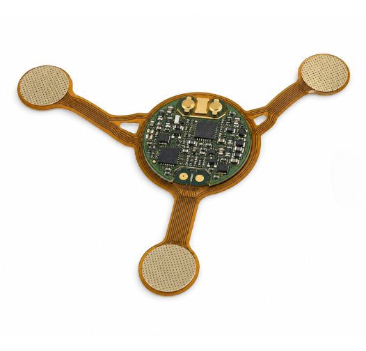
A Wearable Heart Rate Monitor PCB is a specialized circuit board used inside wearable devices to collect, process, and transmit heart rate data. It connects the heart rate sensor with the processor, power system, wireless module, display, and other device functions.
Wearable heart rate monitor PCBs must fit into small and lightweight devices. They also need to handle constant movement, bending, and daily use. Compact layouts, low-power circuits, and reliable sensor connections are important for stable operation.
MedPCB manufactures and assembles PCBs for wearable heart rate monitors and other compact health monitoring devices. We support rigid, flex, and rigid-flex PCB designs, fine-pitch component assembly, and miniature components. Our manufacturing supports prototypes, low-volume production, and volume manufacturing.
Technical Parameter | Manufacturing Capability |
Order Quantity | ≥ 1 PCS, No MOQ |
Board Size | Standard: up to 500 × 600 mm; Advanced: up to 1100 × 500 mm |
Layer Count | Rigid: 1–40 layers; Flex: 1–8 layers; Rigid-Flex: 2–20 layers |
PCB Types | Rigid, Flex, Rigid-Flex, HDI, and ultra-thin PCB |
Assembly | SMT, THT/DIP, and Mixed-Technology |
Component Sourcing | Full, Partial Turnkey, or Consigned; 300,000+ traceable components |
Component Range | 01005 components, fine-pitch ICs, QFN, BGA, sensor packages, and other miniature components |
Placement Accuracy | ±0.035 mm |
Board Thickness | 0.2–10.0 mm |
Surface Finish | ENIG, ENEPIG, HASL, OSP, Immersion Silver/Tin, Soft/Hard Gold |
Impedance Tolerance | ±5 Ω for <50 Ω; ±10% for ≥50 Ω |
Materials | High-Tg FR-4, Polyimide, Rogers, Megtron 6 and other qualified PCB materials |


Challenge: Wearable heart rate monitors have very limited internal space. The PCB must fit around sensors, batteries, displays, and wireless modules. Small components and tight layouts also increase the risk of placement and soldering defects.
MedPCB Solution: We support compact HDI, multilayer, flex, and rigid-flex PCBs with precision assembly. Our SMT lines support components down to 01005 packages and fine-pitch BGA assembly.

Challenge: Wearable heart rate monitor PCBAs may include PPG or ECG sensor interfaces, analog front-end devices, LEDs, photodiodes, and other signal-sensitive components. Small packages and dense placement can increase assembly and soldering risks around these circuits.
MedPCB Solution: MedPCB controls solder paste printing, component placement, polarity, reflow profiles, and cleaning according to the approved assembly requirements. Fine-pitch SMT capability supports miniature sensor and analog components used in compact wearable PCBAs.

Challenge: Wearable devices experience repeated bending, movement, vibration, and contact with the user's skin. Rigid PCBs may not fit well in curved or moving sections of the device.
MedPCB Solution: Our flex and rigid-flex PCB capability supports tight layouts, curved spaces, and repeated movement. We also provide precise SMT assembly and mixed-technology assembly for reliable connections in compact wearable devices.

Challenge: Wearable heart rate monitors can be exposed to sweat, skin moisture, and temperature changes. Moisture can cause corrosion, leakage, or long-term PCB and component reliability issues.
MedPCB Solution: We can provide conformal coating and selective potting where required. Our assembly process also includes controlled soldering, inspection, and electrical testing to help detect assembly defects before shipment.

PCB Inspection & Electrical Testing
We inspect wearable heart rate monitor PCBs during fabrication. Electrical testing checks continuity, isolation, and basic board performance. Dimensional checks verify board size and critical features.
PCBA Process Inspection
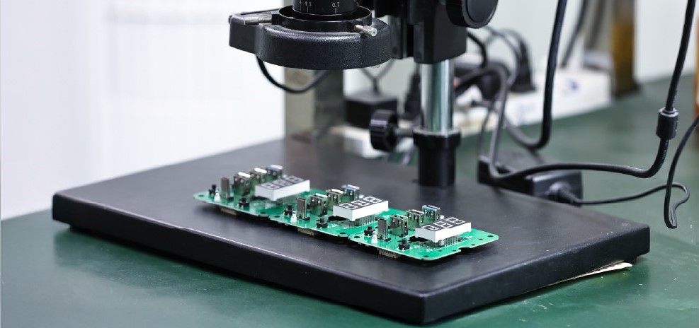
We inspect component placement and solder joints throughout assembly. 3D SPI checks solder paste before component placement. AOI checks component position, polarity, and visible solder defects. 3D X-ray checks hidden joints on BGAs, QFNs, and other dense components.
Functional Testing & Traceability
We perform functional tests based on your approved requirements. Testing can cover power circuits, heart rate sensor interfaces, displays, wireless communication, and other device functions. Production and component records are maintained for traceability.
Need reliable Wearable Heart Rate Monitor PCB & PCBA? Send your Gerber files, BOM, and assembly files for a free DFM/DFA review.
Our Wearable Heart Rate PCB FAQ addresses key questions about PCB manufacturing and assembly requirements. We cover rigid, flex, and rigid-flex PCB fabrication, thin polyimide materials, fine-pitch SMT assembly, low-power sensor circuits, and signal integrity for accurate heart rate monitoring. We also cover ISO 13485 manufacturing, precise component placement, and flexible assembly options from prototypes to volume production. For every wearable heart rate PCB project, we provide controlled fabrication and assembly based on the device size, sensor layout, power requirements, and wearable application.
English
French
German
Japanese
Korean