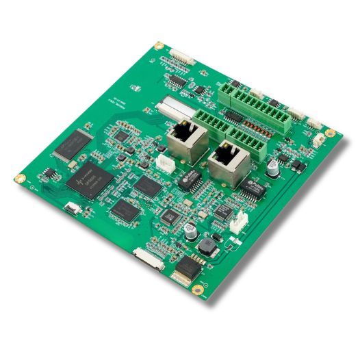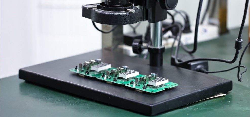
An ultrasound equipment PCB is a specialized circuit board used inside ultrasound machines. It controls key electronic functions, including signal transmission, echo reception, image processing, and system control.
Ultrasound PCBs must provide stable signal transmission and reliable electrical performance. High-speed signals can be sensitive to noise and signal loss. For this reason, the PCB may require controlled impedance, multilayer construction, HDI technology, and suitable high-frequency materials.
The PCB works with the ultrasound transducer to process electrical signals into diagnostic images. Its design and manufacturing quality can affect signal integrity, imaging performance, and overall system reliability.
MedPCB manufactures and assembles ultrasound equipment PCBs for medical imaging systems. We support HDI, multilayer, rigid, and high-frequency PCB designs for prototypes, low-volume production, and volume manufacturing. Our medical PCB manufacturing and assembly follows ISO 13485 and IPC Class 2/3 requirements.
Technical Parameter | Manufacturing Capability |
Order Quantity | ≥ 1 PCS |
Quality Grade | IPC-6012 Class 2 & Class 3 |
Board Size | Standard: up to 500 × 600 mm; Advanced: up to 1100 × 500 mm |
Layer Count | 1–40 layers. Supports multilayer and hybrid stackups for ultrasound equipment |
Assembly Technologies | Surface Mount (SMT), Through-Hole (THT/DIP), and Mixed-Technology |
Component Sourcing | Full Turnkey, Partial Turnkey, or Consigned (access to 300,000+ genuine parts) |
Component Range | From 01005 packages to 0.2 mm fine-pitch BGAs (no maximum component size limit) |
Placement Accuracy | ±0.035 mm via automated component placement |
Board Thickness | 0.2–10.0 mm. Standard: 0.2–3.2 mm; Advanced: 3.4–10.0 mm |
Copper Thickness | 17–350 μm (0.5–10 oz). Standard: 0.5–4 oz |
Min. Trace Width / Spacing | Internal: 3/3 mil (0.075 mm); External: 3/3 mil advanced, 3.5/4 mil standard, depending on copper weight |
Surface Finish | ENIG, ENEPIG, Lead-Free HASL, OSP, Immersion Silver, Immersion Tin, Flash Gold, Hard Gold, Soft Gold, and combination finishes |
Impedance Tolerance | ±5 Ω for <50 Ω; ±10% for ≥50 Ω |
Materials | FR-4, high-Tg materials, high-frequency laminates, and other materials suitable for ultrasound applications |


Challenge - Ultrasound transmit circuits can generate high-voltage pulses that require proper PCB spacing and insulation. Poor clearance or assembly control can increase the risk of electrical failure.
Our Solution - We review creepage, clearance, component spacing, and soldering requirements during DFM/DFA. Controlled assembly processes help maintain the required electrical clearances, insulation, and soldering quality.

Challenge - Ultrasound receive circuits handle weak signals and can be sensitive to electrical noise. Poor grounding, component placement, or soldering can affect signal quality.
Our Solution - We review component placement, grounding, signal routing, and mixed-signal areas before assembly. Precise SMT placement and controlled soldering help maintain stable signal performance.

Challenge - Ultrasound systems often contain many channels and components in a compact space. Fine-pitch packages and dense layouts require accurate component placement and soldering.
Our Solution - We support fine-pitch SMT assembly and high-density PCB designs. SPI, AOI,

Challenge - Medical ultrasound PCBs may use specialized ICs, sensors, connectors, and other components. Component shortages or substitutions can affect production and product consistency.
Our Solution - We source components through qualified suppliers and verify part numbers and specifications through IQC. Approved alternatives can also be reviewed when required to help maintain production continuity.
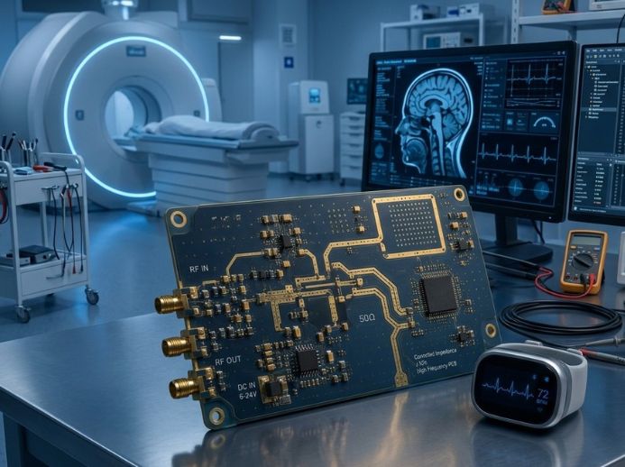
HDI PCB
We manufacture HDI PCBs for compact high-density ultrasound electronics. Our HDI process features fine-line routing and microvias for space-limited designs.
High-Frequency & Low-Loss PCB
We fabricate low-loss PCBs using Rogers, Taconic and similar laminates. Controlled impedance and tight tolerances ensure stable signal transmission for ultrasound circuits.
Rigid-Flex PCB
MedPCB provides rigid-flex PCB manufacturing for ultrasound devices that need flexible connections within compact mechanical assemblies. We control bend areas, layer registration, copper routing, and flex-to-rigid transitions to support reliable connections in handheld probes and space-constrained equipment.
Mixed-Technology PCBA
We perform mixed SMT and through-hole assembly for ultrasound PCBAs with full process quality control. Our production supports BGA, QFN, LGA, and other small-pitch packages, with solder paste inspection, AOI, X-ray inspection, and controlled reflow profiles for reliable solder joints.
MedPCB delivers one‑stop PCB fabrication and assembly services. Send us your inquiry for your ultrasound PCB & PCBA project.
Our Ultrasound Equipment PCB FAQ addresses essential questions regarding your eco-friendly manufacturing requirements. We cover our capabilities for multilayer halogen-free circuits, material selection, thermal stability, strict ISO 13485 quality standards, and compliance with RoHS and REACH regulations. For every medical PCB project, we guarantee high-precision fabrication tailored for critical healthcare applications.
Yes, MedPCB supports the full product lifecycle, transitioning seamlessly from initial rapid prototyping and New Product Introduction (NPI) to scalable high-volume production with consistent quality and optimized costs.
English
French
German
Japanese
Korean