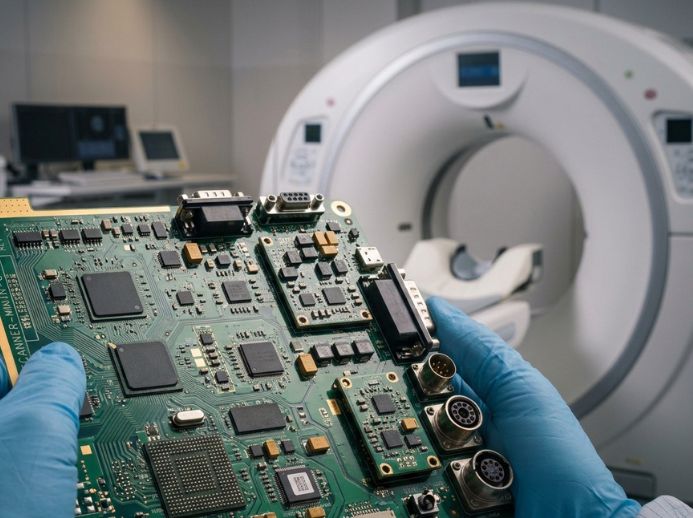
A medical CT scanner PCB is a specialized circuit board used inside Computed Tomography (CT) imaging systems. It supports key functions such as data acquisition, power distribution, signal processing, and system control.
CT scanner PCBs demand stable electrical performance and long-term reliability. Depending on circuit functions, they adopt multilayer structures, fine-line routing, controlled impedance and HDI for high-speed imaging data capture and processing.
CT equipment works under harsh electrical, thermal and mechanical conditions. These PCBs are widely used in imaging control, detector interfaces, high-speed data processing and precision power circuits.
MedPCB offers full PCB fabrication and PCBA assembly services for CT scanner PCB, from prototypes to mass production. We manufacture HDI and complex multilayer rigid boards to meet your CT project requirements.
Medical CT scanner PCBs handle large amounts of imaging data at high speed. Controlled impedance, stable stackup construction, accurate routing, and consistent component placement help maintain predictable electrical performance.
Technical Parameter | CT Scanner PCB Manufacturing Capability |
Board Size | Standard: up to 500 × 600 mm Advanced: up to 1100 × 500 mm |
Layer Count | 1–40 layers Standard: 1–20 layers Advanced: 22–40 layers, including hybrid stackups |
Assembly Technologies | Surface Mount (SMT), Through-Hole (THT/DIP), and Mixed-Technology |
Component Sourcing | Full Turnkey, Partial Turnkey, or Consigned (access to 300,000+ genuine parts) |
Component Range | From 01005 packages to 0.2 mm fine-pitch BGAs (no maximum component size limit) |
Placement Accuracy | ±0.035 mm via automated component placement |
Board Thickness | 0.2–10.0 mm Standard: 0.2–3.2 mm Advanced: 3.4–10.0 mm |
Min. Trace Width / Spacing | Internal: 3/3 mil (0.075 mm)External: 3/3 mil advanced; 3.5/4 mil standard, depending on copper weight |
Surface Finish | ENIG, ENEPIG, Lead-Free HASL, OSP, Immersion Silver, Immersion Tin, Flash Gold, Hard Gold, Soft Gold, and combination finishes |
Impedance Tolerance | ±5 Ω for <50 Ω±10% for ≥50 Ω |
PCB Materials | FR-4, High-Tg FR-4, Rogers, and other advanced materials based on CT scanner design requirements |
PCB Types | Multilayer, HDI, rigid, and hybrid PCB constructions |


Challenge: CT scanners process large amounts of imaging data at high speeds. High-frequency signals require controlled impedance, precise trace geometry, and stable dielectric properties. Small changes in the PCB stackup or routing can affect signal quality.
Our Solution: We review impedance requirements during the engineering and DFM process. Our fabrication controls trace width, spacing, copper thickness, and dielectric thickness to support stable signal transmission across complex multilayer CT scanner PCBs.

Challenge: CT scanner PCBs operate near high-power components, processors, and power circuits that generate significant heat. Poor thermal management can increase component temperatures and affect long-term PCB reliability.
Our Solution: We select suitable PCB materials and components, copper weights, and thermal structures based on the design requirements. Thermal vias, copper planes, and heavy-copper sections can also be incorporated to improve heat dissipation.

Challenge: CT scanner electronics often require compact layouts with high component density. Fine-pitch BGAs, microvias, buried vias, and fine traces can make fabrication and registration more demanding.
Our Solution: We support HDI fabrication and assembly with laser-drilled microvias, fine-line traces, and sequential lamination. Our engineering team reviews the stackup, via structures, BOM, and component land patterns before production to reduce manufacturing and assembly risks.

Challenge: CT scanner assemblies may use specialized ICs, sensors, connectors, and other components with long lead times or limited availability. Component substitutions can also affect the electrical and mechanical performance of the final assembly.
Our Solution: We work with approved BOMs and customer-specified components whenever required. Our sourcing team checks component availability and specifications during the assembly process. When an alternative is needed, we can provide the relevant part information for customer approval before production.

HDI PCB
We produce HDI PCBs with fine traces and laser microvias to deliver compact high-density layouts for complex CT imaging circuits.
High-Tg PCB
MedPCB fabricates multilayer CT boards using high-Tg laminates that withstand continuous thermal cycling and maintain stable performance.
Rigid-Flex PCB
We manufacture rigid-flex PCBs to reduce connectors and save internal space within compact CT scanner modules.
Fine-Pitch PCBA
MedPCB assemble BGA, QFN, and fine-pitch components, using precision SMT plus 3D SPI, AOI and X-ray inspection for dependable soldering.
MedPCB provides free DFM review and IPC Class 2/3 manufacturing for medical PCB projects. Our engineering team can review your CT scanner PCB or PCBA design. Just send us your project details today!
Our Medical CT Scanner PCB FAQ addresses essential questions regarding your eco-friendly manufacturing requirements. We cover our capabilities for multilayer halogen-free circuits, material selection, thermal stability, strict ISO 13485 quality standards, and compliance with RoHS and REACH regulations. For every medical PCB project, we guarantee high-precision fabrication tailored for critical healthcare applications.
English
French
German
Japanese
Korean