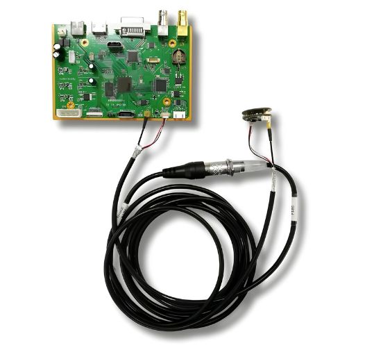
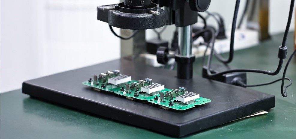
A medical endoscope PCB is a specialized circuit board used inside medical endoscopes and imaging systems. It supports key electronic functions, including image capture, LED illumination, image signal processing, power management, and device control.
Medical endoscope PCBs must handle high-speed image signals while maintaining stable electrical performance. The PCB also needs compact construction, low noise, reliable signal transmission, and precise component placement. Small endoscope designs may require HDI, fine-pitch components, flexible circuits, or rigid-flex PCB construction.
MedPCB manufactures and assembles medical-grade PCBs for medical endoscopes. We support rigid, flex, rigid-flex, HDI, and multilayer PCB designs. Our manufacturing supports prototypes, low-volume production, and volume manufacturing.
|
Technical Parameter |
Manufacturing Capability |
|
Order Quantity |
≥ 1 PCS, No MOQ |
|
Board Size |
Standard: up to 500 × 600 mm; Advanced: up to 1100 × 500 mm |
|
Layer Count |
Rigid PCB: 1–40 layers Rigid Flex PCB: Standard: 2–12 layers (up to 10 flex layers), Advanced: 13–20 layers (up to 18 flex layers) |
|
Assembly Technologies |
Surface Mount (SMT), Through-Hole (THT/DIP), and Mixed-Technology |
|
Component Sourcing |
Full Turnkey, Partial Turnkey, or Consigned (access to 300,000+ genuine parts) |
|
Component Range |
From 01005 packages to 0.2 mm fine-pitch BGAs |
|
Placement Accuracy |
±0.035 mm via automated component placement |
|
Board Thickness |
0.2–10.0 mm (Standard: 0.2–3.2 mm; Advanced: 3.4–10.0 mm) |
|
Min. Trace Width / Spacing |
Internal: 3/3 mil (0.075 mm); External: 3/3 mil advanced, 3.5/4 mil standard |
|
Surface Finish |
ENIG, ENEPIG, Lead-Free HASL, OSP, Immersion Silver, Immersion Tin, Soft/Hard Gold, |
|
Impedance Tolerance |
±5 Ω for <50 Ω; ±10% for ≥50 Ω |
|
Materials |
High-Tg FR-4, Polyimide (Flex), Rogers, Megtron 6, and Other Qualified PCB Materials |

We review your medical endoscope PCB design before production. Our engineers check the layout, pad design, trace spacing, impedance requirements, component placement, flex or rigid-flex structure, and assembly details. This helps identify potential manufacturing issues early.

Challenge: Medical endoscopes use flex and rigid-flex PCBs in the distal tip, insertion tube, handle, and processor sections. These areas undergo repeated bending and movement. The rigid-to-flex transition can experience high mechanical stress, especially during scope articulation.
Our Solution: MedPCB manufactures flex and rigid-flex PCBs with controlled transition areas. Stiffeners can support component and connector zones, while gradual trace fan-out helps reduce stress. Controlled fabrication also supports reliable rigid-flex connections and consistent mechanical performance.

Challenge: The endoscope tip has very limited space for the CMOS image sensor, LEDs, timing and communication circuits, and other components. Designs may require HDI, multilayer construction and 01005 components.
Our Solution: MedPCB manufactures HDI, multilayer, flex, rigid, and rigid-flex PCBs for compact endoscope designs. We support ultra-fine pitch SMT from 01005 packages to 0.2 mm BGAs. AOI, 3D X-ray, and electrical testing help verify high-density assemblies.

Challenge: Endoscope electronics may use high-speed image and communication interfaces across compact rigid, flex, or rigid-flex circuits. These designs can require tight control of trace geometry, stackup, and impedance during PCB fabrication.
Our Solution: MedPCB manufactures controlled-impedance PCBs according to the approved stackup and impedance requirements. We control material selection, copper thickness, trace geometry, dielectric thickness, and fabrication tolerances, with impedance testing available when specified.

Challenge: Compact endoscope PCBAs can have dense component spacing and signal-sensitive areas where flux residue, contamination, or improper cleaning may affect assembly quality. Some applications may also require additional protection against moisture or environmental exposure.
Our Solution: MedPCB controls cleaning and handling according to the approved assembly requirements. Cleanliness inspection, conformal coating, and encapsulation can be provided when specified by the product design and environmental requirements.

PCB Inspection & Electrical Testing
We inspect your endoscope PCBs throughout fabrication using AOI, dimensional inspection, and electrical testing. Controlled-impedance testing can also be performed when required by your design.
PCBA Process Inspection
We inspect component placement, solder joints, and assembly quality during the PCBA process. 3D SPI checks solder paste volume and placement before component assembly. AOI verifies component position, polarity, solder joints, and other visible defects. X-ray inspection can check hidden solder joints on BGAs, QFNs, and other high-density components.
Functional Testing & Traceability
We perform functional testing based on your approved test requirements. Tests can verify power circuits, communication interfaces, image signal paths, LED illumination, and other endoscope functions. Production records and component information are maintained for lot traceability and quality control.
Need reliable Medical Endoscope PCB & PCBA? Send your Gerber files, BOM, and assembly files to sales@medicalpcb.com for a free DFM/DFA review.
Our Medical Endoscope PCB FAQ covers key questions about endoscope PCB manufacturing and assembly. We explain our capabilities for compact, high-precision circuits, rigid, flex, and rigid-flex PCBs, material selection, miniature component assembly, and strict ISO 13485 quality standards. We also cover RoHS and REACH compliance, testing, and reliability requirements for medical imaging and diagnostic devices.
English
French
German
Japanese
Korean